ZHCSFK8B September 2016 – October 2017 TAS6424-Q1
PRODUCTION DATA.
- 1 特性
- 2 应用
- 3 说明
- 4 修订历史记录
- 5 Device Comparison Table
- 6 Pin Configuration and Functions
- 7 Specifications
- 8 Parameter measurement Information
-
9 Detailed description
- 9.1 Overview
- 9.2 Functional Block Diagram
- 9.3
Feature Description
- 9.3.1 Serial Audio Port
- 9.3.2 High-Pass Filter
- 9.3.3 Volume Control and Gain
- 9.3.4 High-Frequency Pulse-Width Modulator (PWM)
- 9.3.5 Gate Drive
- 9.3.6 Power FETs
- 9.3.7 Load Diagnostics
- 9.3.8
Protection and Monitoring
- 9.3.8.1 Overcurrent Limit (ILIMIT)
- 9.3.8.2 Overcurrent Shutdown (ISD)
- 9.3.8.3 DC Detect
- 9.3.8.4 Clip Detect
- 9.3.8.5 Global Overtemperature Warning (OTW), Overtemperature Shutdown (OTSD)
- 9.3.8.6 Channel Overtemperature Warning [OTW(i)] and Shutdown [OTSD(i)]
- 9.3.8.7 Undervoltage (UV) and Power-On-Reset (POR)
- 9.3.8.8 Overvoltage (OV) and Load Dump
- 9.3.9 Power Supply
- 9.3.10 Hardware Control Pins
- 9.4 Device Functional Modes
- 9.5 Programming
- 9.6
Register Maps
- 9.6.1 Mode Control Register (address = 0x00) [default = 0x00]
- 9.6.2 Miscellaneous Control 1 Register (address = 0x01) [default = 0x32]
- 9.6.3 Miscellaneous Control 2 Register (address = 0x02) [default = 0x62]
- 9.6.4 SAP Control (Serial Audio-Port Control) Register (address = 0x03) [default = 0x04]
- 9.6.5 Channel State Control Register (address = 0x04) [default = 0x55]
- 9.6.6 Channel 1 Through 4 Volume Control Registers (address = 0x05-0x088) [default = 0xCF]
- 9.6.7 DC Load Diagnostic Control 1 Register (address = 0x09) [default = 0x00]
- 9.6.8 DC Load Diagnostic Control 2 Register (address = 0x0A) [default = 0x11]
- 9.6.9 DC Load Diagnostic Control 3 Register (address = 0x0B) [default = 0x11]
- 9.6.10 DC Load Diagnostic Report 1 Register (address = 0x0C) [default = 0x00]
- 9.6.11 DC Load Diagnostic Report 2 Register (address = 0x0D) [default = 0x00]
- 9.6.12 DC Load Diagnostics Report 3—Line Output—Register (address = 0x0E) [default = 0x00]
- 9.6.13 Channel State Reporting Register (address = 0x0F) [default = 0x55]
- 9.6.14 Channel Faults (Overcurrent, DC Detection) Register (address = 0x10) [default = 0x00]
- 9.6.15 Global Faults 1 Register (address = 0x11) [default = 0x00]
- 9.6.16 Global Faults 2 Register (address = 0x12) [default = 0x00]
- 9.6.17 Warnings Register (address = 0x13) [default = 0x20]
- 9.6.18 Pin Control Register (address = 0x14) [default = 0xFF]
- 9.6.19 AC Load Diagnostic Control 1 Register (address = 0x15) [default = 0x00]
- 9.6.20 AC Load Diagnostic Control 2 Register (address = 0x16) [default = 0x00]
- 9.6.21 AC Load Diagnostic Impedance Report Ch1 through CH4 Registers (address = 0x17-0x1A) [default = 0x00]
- 9.6.22 AC Load Diagnostic Phase Report High Register (address = 0x1B) [default = 0x00]
- 9.6.23 AC Load Diagnostic Phase Report Low Register (address = 0x1C) [default = 0x00]
- 9.6.24 AC Load Diagnostic STI Report High Register (address = 0x1D) [default = 0x00]
- 9.6.25 AC Load Diagnostic STI Report Low Register (address = 0x1C) [default = 0x00]
- 9.6.26 Miscellaneous Control 3 Register (address = 0x21) [default = 0x00]
- 9.6.27 Clip Control Register (address = 0x22) [default = 0x01]
- 9.6.28 Clip Window Register (address = 0x23) [default = 0x14]
- 9.6.29 Clip Warning Register (address = 0x24) [default = 0x00]
- 9.6.30 ILIMIT Status Register (address = 0x25) [default = 0x00]
- 9.6.31 Miscellaneous Control 4 Register (address = 0x26) [default = 0x40]
- 10Application and Implementation
- 11Power Supply Recommendations
- 12Layout
- 13器件和文档支持
- 14机械、封装和可订购信息
7 Specifications
7.1 Absolute Maximum Ratings
over operating free-air temperature range (unless otherwise noted)| MIN | MAX | UNIT | |||
|---|---|---|---|---|---|
| PVDD, VBAT | DC supply voltage relative to GND | –0.3 | 30 | V | |
| VMAX | Transient supply voltage: PVDD, VBAT | t ≤ 400 ms exposure | –1 | 40 | V |
| VRAMP | Supply-voltage ramp rate: PVDD, VBAT | 75 | V/ms | ||
| VDD | DC supply voltage relative to GND | –0.3 | 3.5 | V | |
| IMAX | Maximum current per pin (PVDD, VBAT, OUT_xP, OUT_xM, GND) | 8 | A | ||
| IMAX_PULSED | Pulsed supply current per PVDD pin (one shot) | t < 100 ms | 12 | A | |
| VLOGIC | Input voltage for logic pins (SCL, SDA, SDIN1, SDIN2, MCLK, BCLK, LRCLK, MUTE, STANDBY, I2C_ADDRx) | –0.3 | VDD + 0.5 | V | |
| VGND | Maximum voltage between GND pins | –0.3 | 0.3 | V | |
| TJ | Maximum operating junction temperature | –55 | 150 | °C | |
| Tstg | Storage temperature | –55 | 150 | °C | |
7.2 ESD Ratings
| VALUE | UNIT | ||||
|---|---|---|---|---|---|
| V(ESD) | Electrostatic discharge | Human-body model (HBM), per AEC Q100–002(1) | ±3000 | V | |
| Charged-device model (CDM), per AEC Q100–011 | All pins | ±500 | |||
| Corner pins (1, 28, 29 and 56) | ±1000 | ||||
(1) AEC Q100–002 indicates that HBM stressing shall be in accordance with the ANSI/ESDA/JEDEC JS–001 specification.
7.3 Recommended Operating Conditions
| MIN | NOM | MAX | UNIT | |||
|---|---|---|---|---|---|---|
| PVDD | Output FET supply voltage | Relative to GND | 4.5 | 26.4 | V | |
| VBAT | Battery supply voltage input | Relative to GND | 4.5 | 14.4 | 18 | V |
| VDD | DC logic supply | Relative to GND | 3.0 | 3.3 | 3.5 | V |
| TA | Ambient temperature | –40 | 125 | °C | ||
| TJ | Junction temperature | An adequate thermal design is required | –40 | 150 | °C | |
| RL | Nominal speaker load impedance | BTL Mode | 2 | 4 | Ω | |
| PBTL Mode | 1 | 2 | ||||
| RPU_I2C | I2C pullup resistance on SDA and SCL pins | 1 | 4.7 | 10 | kΩ | |
| CBypass | External capacitance on bypass pins | Pin 2, 3, 5, 6, 8, 9, 10, 19 | 1 | µF | ||
| COUT | External capacitance to GND on OUT pins | Limit set by DC-diagnostic timing | 1 | 3.3 | µF | |
| LO | Output filter inductance | Minimum inductance at ISD current levels | 1 | µH | ||
7.4 Thermal Information
| THERMAL METRIC(1) | TAS6424-Q1(2) | TAS6424-Q1(3) | UNIT | |
|---|---|---|---|---|
| DKQ (HSSOP) | DKQ (HSSOP) | |||
| 56 PINS | 56 PINS | |||
| RθJA | Junction-to-ambient thermal resistance | — | — | °C/W |
| RθJC(top) | Junction-to-case (top) thermal resistance | 0.7 | 1.1 | °C/W |
| RθJB | Junction-to-board thermal resistance | — | — | °C/W |
| ψJT | Junction-to-top characterization parameter | — | — | °C/W |
| ψJB | Junction-to-board characterization parameter | 10 | 10 | °C/W |
| RθJC(bot) | Junction-to-case (bottom) thermal resistance | — | — | °C/W |
(1) For more information about traditional and new thermal metrics, see the Semiconductor and IC Package Thermal Metrics application report (SPRA953).
(2) JEDEC Standard 4 Layer PCB.
(3) Measured using the TAS6424-Q1 EVM layout and heat sink. The device is not intended to be used without a heat sink.
7.5 Electrical Characteristics
Test conditions (unless otherwise noted): TC = 25°C, PVDD = VBAT = 14.4 V, VDD = 3.3 V, RL = 4 Ω, Pout = 1 W/ch, ƒ = 1 kHz, fSW = 2.11 MHz, AES17 Filter, default I2C settings, see Figure 79 and Figure 82| PARAMETER | TEST CONDITIONS | MIN | TYP | MAX | UNIT | |
|---|---|---|---|---|---|---|
| OPERATING CURRENT | ||||||
| IPVDD_IDLE | PVDD idle current | All channels playing, no audio input | 75 | 90 | mA | |
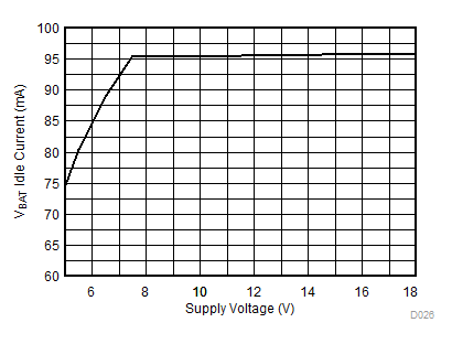
| IVBAT_IDLE | VBAT idle current | All channels playing, no audio input | 90 | 100 | mA | |
| IPVDD_STBY | PVDD standby current | STANDBYActive, VDD = 0 V | 1 | 10 | μA | |
| IVBAT_STBY | VBAT standby current | STANDBYActive, VDD = 0 V | 4 | 10 | μA | |
| IVDD | VDD supply current | All channels playing, –60-dB signal | 15 | 18 | mA | |
| OUTPUT POWER | ||||||
| PO_BTL | Output power per channel, BTL | 4 Ω, PVDD = 14.4 V, THD+N = 1%, TC = 75°C | 20 | 22 | W | |
| 4 Ω, PVDD = 14.4 V, THD+N = 10%, TC = 75°C | 25 | 27 | ||||
| 2 Ω, PVDD = 14.4 V, THD+N = 1%, TC = 75°C | 38 | 40 | ||||
| 2 Ω, PVDD = 14.4 V, THD+N = 10%, TC = 75°C | 42 | 45 | ||||
| 4 Ω, PVDD = 25 V, THD+N = 1%, TC = 75°C | 50 | 55 | ||||
| 4 Ω, PVDD = 25 V, THD+N = 10%, TC = 75°C | 70 | 75 | ||||
| PO_PBTL | Output power per channel in parallel mode, PBTL | 2 Ω, PVDD = 14.4 V, THD+N = 1%, TC = 75°C | 35 | 40 | W | |
| 2 Ω, PVDD = 14.4 V, THD+N = 10%, TC = 75°C | 45 | 50 | ||||
| 1 Ω, PVDD = 14.4 V, THD+N = 1%, TC = 75°C | 72 | 80 | ||||
| 1 Ω, PVDD = 14.4 V, THD+N = 10%, TC = 75°C | 80 | 90 | ||||
| 2 Ω, PVDD = 25 V, THD+N = 1%, TC = 75°C | 98 | 120 | ||||
| 2 Ω, PVDD = 25 V, THD+N = 10%, TC = 75°C | 138 | 150 | ||||
| EFFP | Power efficiency | 4 channels operating, 25-W output power/ch 4-Ω load, PVDD = 14.4 V, TC = 25°C, including indcutor losses(1) | 86% | |||
| AUDIO PERFORMANCE | ||||||
| Vn | Output noise voltage | Zero input, A-weighting, gain level 1, PVDD = 14.4 V | 42 | μV | ||
| Zero input, A-weighting, gain level 2, PVDD = 14.4 V | 55 | |||||
| Zero input, A-weighting, gain level 3, PVDD = 18 V | 67 | |||||
| Zero input, A-weighting, gain level 4, PVDD = 25 V | 85 | |||||
| GAIN | Peak output voltage/dBFS | Gain level 1, Register 0x01, bit 1-0 = 00 | 7.5 | V/FS | ||
| Gain level 2, Register 0x01, bit 1-0 = 01 | 15 | |||||
| Gain level 3, Register 0x01, bit 1-0 = 10 | 21 | |||||
| Gain level 4, Register 0x01, bit 1-0 = 11 | 29 | |||||
| Crosstalk | Channel crosstalk | PVDD = 14.4 Vdc + 1 VRMS, ƒ = 1 kHz | –90 | –75 | dB | |
| PSRR | Power-supply rejection ratio | PVDD = 14.4 Vdc + 1 VRMS, ƒ = 1 kHz | 75 | dB | ||
| THD+N | Total harmonic distortion + noise | 0.02% | 0.05% | |||
| GCH | Channel-to-channel gain variation | –0.5 | 0 | 0.5 | dB | |
| LINE OUTPUT PERFORMANCE | ||||||
| Vn_LINEOUT | LINE output noise voltage | Zero input, A-weighting, channel set to LINE MODE | 42 | μV | ||
| VO_LINEOUT | LINE output voltage | 0-dB input, channel set to LINE MODE | 5.5 | VRMS | ||
| THD+N | Line output total harmonic distortion + noise | VO = 2 VRMS , channel set to LINE MODE | 0.01% | 0.03% | ||
| DIGITAL INPUT PINS | ||||||
| VIH | Input logic level high | 70 | %VDD | |||
| VIL | Input logic level low | 30 | %VDD | |||
| IIH | Input logic current, high | VI = VDD | 15 | µA | ||
| IIL | Input logic current, low | VI = 0 | –15 | µA | ||
| PWM OUTPUT STAGE | ||||||
| RDS(on) | FET drain-to-source resistance | Not including bond wire and package resistance | 90 | mΩ | ||
| OVERVOLTAGE (OV) PROTECTION | ||||||
| VPVDD_OV | PVDD overvoltage shutdown | 27.0 | 27.8 | 28.8 | V | |
| VPVDD_OV_HYS | PVDD overvoltage shutdown hysteresis | 0.8 | V | |||
| VVBAT_OV | VBAT overvoltage shutdown | 19.3 | 20 | 22 | V | |
| VVBAT_OV_HYS | VBAT overvoltage shutdown hysteresis | 0.6 | V | |||
| UNDERVOLTAGE (UV) PROTECTION | ||||||
| VBATUV | VBAT undervoltage shutdown | 4 | 4.5 | V | ||
| VBATUV_HYS | VBAT undervoltage shutdown hysteresis | 0.2 | V | |||
| PVDDUV | PVDD undervoltage shutdown | 4 | 4.5 | V | ||
| PVDDUV_HYS | PVDD undervoltage shutdown hysteresis | 0.2 | V | |||
| BYPASS VOLTAGES | ||||||
| VGVDD | Gate drive bypass pin voltage | 7 | V | |||
| VAVDD | Analog bypass pin voltage | 6 | V | |||
| VVCOM | Common bypass pin voltage | 2.5 | V | |||
| VVREG | Regulator bypass pin voltage | 5.5 | V | |||
| POWER-ON RESET (POR) | ||||||
| VPOR | VDD voltage for POR | 2.1 | 2.7 | V | ||
| VPOR_HY | VDD POR recovery hysteresis voltage | 0.5 | V | |||
| OVERTEMPERATURE (OT) PROTECTION | ||||||
| OTW(i) | Channel overtemperature warning | 150 | °C | |||
| OTSD(i) | Channel overtemperature shutdown | 175 | °C | |||
| OTW | Global junction overtemperature warning | Set by register 0x01 bit 5-6, default value | 130 | °C | ||
| OTSD | Global junction overtemperature shutdown | 160 | °C | |||
| OTHYS | Overtemperature hysteresis | 15 | °C | |||
| LOAD OVER CURRENT PROTECTION | ||||||
| ILIM | Overcurrent cycle-by-cycle limit | OC Level 1 | 4 | 4.8 | A | |
| OC Level 2 | 6 | 6.5 | ||||
| ISD | Overcurrent shutdown | OC Level 1, Any short to supply, ground, or other channels | 7 | A | ||
| OC Level 2, Any short to supply, ground, or other channels | 9 | |||||
| MUTE MODE | ||||||
| GMUTE | Output attenuation | 100 | dB | |||
| CLICK AND POP | ||||||
| VCP | Output click and pop voltage | ITU-R 2k filter, High-Z/MUTE to Play, Play to Mute/High-Z | 7 | mV | ||
| DC OFSET | ||||||
| VOFFSET | Output offset voltage | 2 | 5 | mV | ||
| DC DETECT | ||||||
| DCFAULT | Output DC fault protection | 2 | 2.5 | V | ||
| DIGITAL OUTPUT PINS | ||||||
| VOH | Output voltage for logic level high | I = ±2 mA | 90 | %VDD | ||
| VOL | Output voltage for logic level low | I = ±2 mA | 10 | %VDD | ||
| tDELAY_CLIPDET | Signal delay when output clipping detected | 20 | μs | |||
| LOAD DIAGNOSTICS | ||||||
| S2P | Maximum resistance to detect a short from OUT pins to PVDD | 500 | Ω | |||
| S2G | Maximum resistance to detect a short from OUT pins to ground | 200 | Ω | |||
| SL | Shorted load detection tolerance | Other channels in Hi-Z | ±0.5 | Ω | ||
| OL | Open load | Other channels in Hi-Z | 40 | 70 | Ω | |
| TDC_DIAG | DC diagnostic time | All 4 Channels | 230 | ms | ||
| LO | Line output | 6 | kΩ | |||
| TLINE_DIAG | Line output diagnostic time | 40 | ms | |||
| ACIMP | AC impedance accuracy | Gain linearity, ƒ = 19 kHz, RL = 2 Ω to 16 Ω, | 25% | |||
| Offset | ±0.5 | Ω | ||||
| TAC_DIAG | AC diagnostic time | All 4 Channels | 520 | ms | ||
| I2C_ADDR PINS | ||||||
| tI2C_ADDR | Time delay needed for I2C address set-up | 300 | μs | |||
- Tested with Output Inductor DFEG7030D-3R3M.
7.6 Timing Requirements
Test conditions (unless otherwise noted): TC = 25 °C, PVDD = VBAT = 14.4 V, VDD = 3.3 V, RL = 4 Ω, PO = 1 W/ch, ƒ = 1 kHz, fSW = 2.11 MHz, AES17 Filter, default I2C settings, see Figure 79 and Figure 82| MIN | TYP | MAX | UNIT | |||
|---|---|---|---|---|---|---|
| I2C CONTROL PORT (See Figure 42) | ||||||
| tBUS | Bus free time between start and stop conditions | 1.3 | μs | |||
| tHOLD1 | Hold time, SCL to SDA | 0 | ns | |||
| tHOLD2 | Hold time, start condition to SCL | 0.6 | μs | |||
| tSTART | I2C startup time after VDD power on reset | 12 | ms | |||
| tRISE | Rise time, SCL and SDA | 300 | ns | |||
| tFALL | Fall time, SCL and SDA | 300 | ns | |||
| tSU1 | Setup, SDA to SCL | 100 | ns | |||
| tSU2 | Setup, SCL to start condition | 0.6 | μs | |||
| tSU3 | Setup, SCL to stop condition | 0.6 | μs | |||
| tW(H) | Required pulse duration SCL High | 0.6 | μs | |||
| tW(L) | Required pulse duration SCL Low | 1.3 | μs | |||
| SERIAL AUDIO PORT (See Figure 36) | ||||||
| DMCLK, DSCLK | Allowable input clock duty cycle | 45% | 50% | 55% | ||
| ƒMCLK | Supported MCLK frequencies: 128, 256, or 512 | 128 | 512 | xFS | ||
| ƒMCLK_Max | Maximum frequency | 25 | MHz | |||
| tSCY | SCLK pulse cycle time | 40 | ns | |||
| tSCL | SCLK pulse-with LOW | 16 | ns | |||
| tSCH | SCLK pulse-with HIGH | 16 | ns | |||
| trise/fall | Rise and fall time | 4 | ns | |||
| tSF | SCLK rising edge to FSYNC edge | 8 | ns | |||
| tFS | FSYNC rising edge to SCLK edge | 8 | ns | |||
| tDS | DATA set-up time | 8 | ns | |||
| tDH | DATA hold time | 8 | ns | |||
| ci | Input capacitance, pins MCLK, SCLK, FSYNC, SDIN1, SDIN2 | 10 | pF | |||
| TLA | Latency from input to output measured in FSYNC sample count | FSYNC = 44.1 kHz or 48 kHz | 30 | |||
| FSYNC = 96 kHz | 12 | |||||
7.7 Typical Characteristics
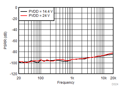
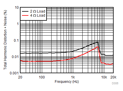
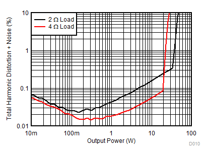
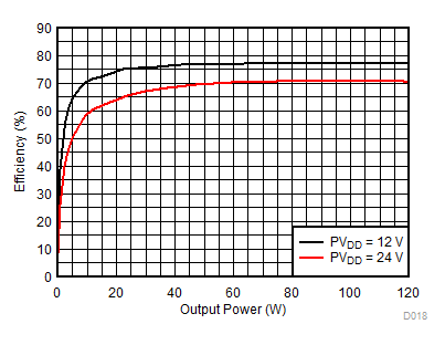
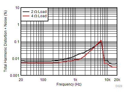
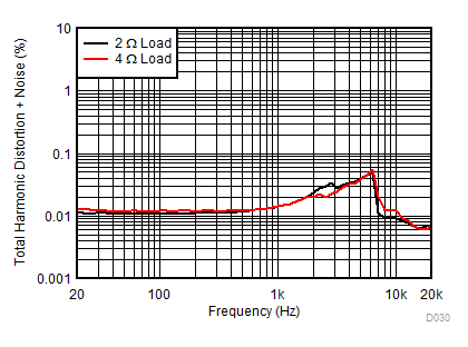
TA = 25 ºC, VVDD = 3.3 V, VBAT = PVDD = 14.4 V, RL = 4 Ω, fIN = 1 kHz, fs = 48 kHz, fSW = 2.11 MHz, AES17 filter, default I2C settings, see Figure 79 and Figure 82 (unless otherwise noted)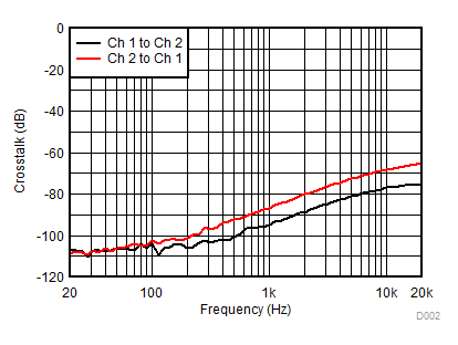
| PO = 1 W |
| PO = 1 W |
| PO = 1 W | 2.11-MHz fSW |

| PO = 1 W | 24 V | 2.11-MHz fSW |
| 2.11-MHz fSW |
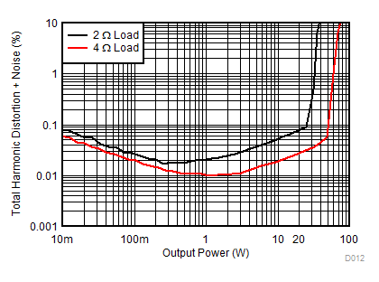
| 24 V | 2.11-MHz fSW |
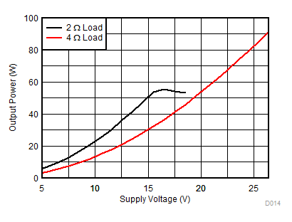
| 10% THD | 2.11-MHz fSW |
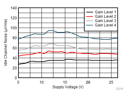
| A-weighted Noise | 2.11-MHz fSW |
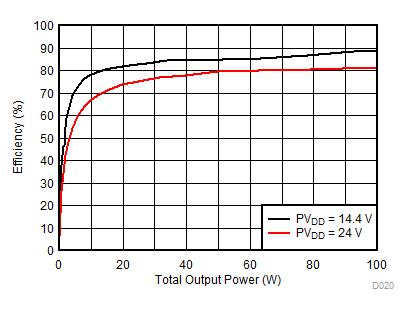
| 4 Ω | 2.1-MHz fSW |
| 2 Ω | 2.1-MHz fSW |
| 1 W | 384-kHz fSW |
| PO = 1 W | 384-kHz fSW | 24-V PVDD |
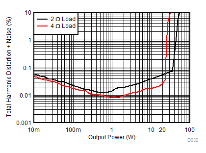
| 384-kHz fSW |
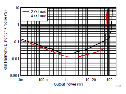
| 384-kHz fSW |
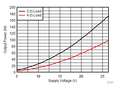
| 384-kHz fSW |
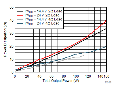
| 384-kHz fSW |
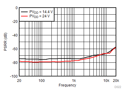
| PO = 1 W |
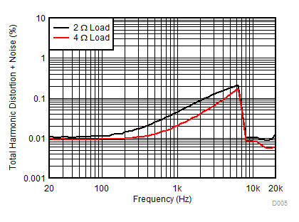
| PO = 1 W | 384-kHz fSW |
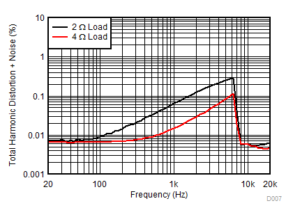
| PO = 1 W | 24 V | 384-kHz fSW |
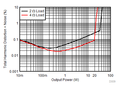
| 384-kHz fSW |
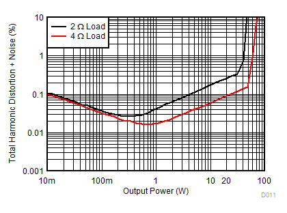
| 24 V | 384-kHz fSW |
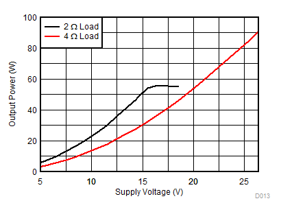
| 10% THD | 384-kHz fSW |
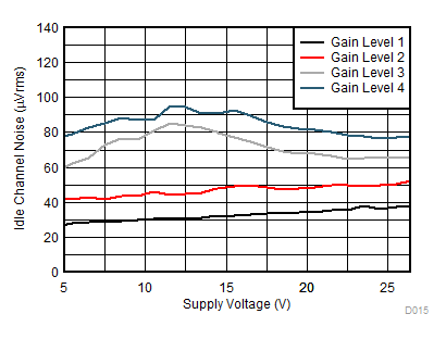
| A-weighted Noise | 384-kHz fSW |
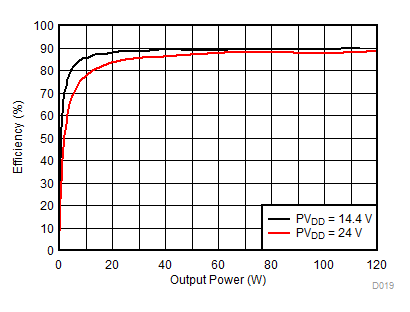
| 4 Ω | 384-kHz fSW |
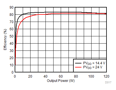
| 2 Ω | 384-kHz fSW |
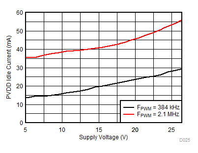
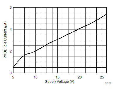
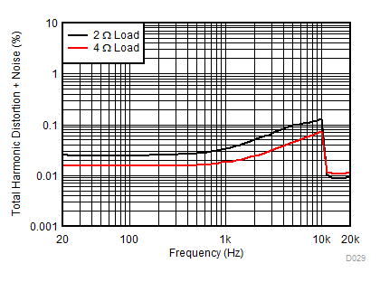
| PO = 1 W | 2.1-MHz fSW |
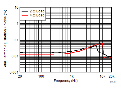
| Po = 1 W | 2.1-MHz fSW | 24-V PVDD |
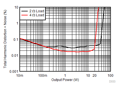
| 2.1-MHz fSW |
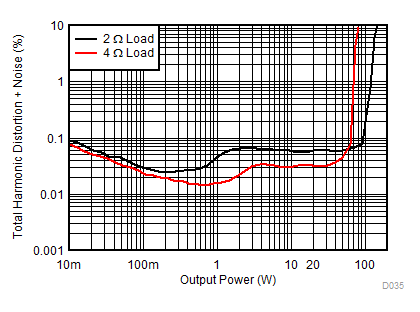
| 2.1-MHz fSW | 24-V PVDD |
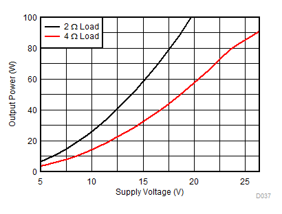
| 2.1-MH fSW |
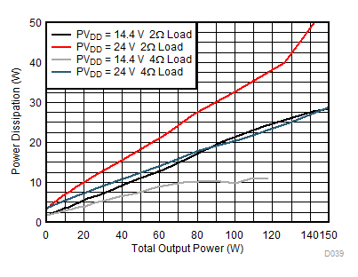
| 2.1-MHz fSW |