ZHCSEH3B December   2015  – September 2018 TAS5411-Q1

PRODUCTION DATA.  

  1. 特性
  2. 应用
  3. 说明
    1.     Device Images
      1.      简化框图
      2.      效率
  4. 修订历史记录
  5. Device Comparison Table
  6. Pin Configuration and Functions
    1.     Pin Functions
  7. Specifications
    1. 7.1 Absolute Maximum Ratings
    2. 7.2 ESD Ratings
    3. 7.3 Recommended Operating Conditions
    4. 7.4 Thermal Information
    5. 7.5 Electrical Characteristics
    6. 7.6 Timing Requirements for I2C Interface Signals
    7. 7.7 Typical Characteristics
  8. Parameter Measurement Information
  9. Detailed Description
    1. 9.1 Overview
    2. 9.2 Functional Block Diagram
    3. 9.3 Feature Description
      1. 9.3.1 Analog Audio Input and Preamplifier
      2. 9.3.2 Pulse-Width Modulator (PWM)
      3. 9.3.3 Gate Drive
      4. 9.3.4 Power FETs
      5. 9.3.5 Load Diagnostics
        1. 9.3.5.1 Load Diagnostics Sequence
        2. 9.3.5.2 Faults During Load Diagnostics
      6. 9.3.6 Protection and Monitoring
      7. 9.3.7 I2C Serial Communication Bus
        1. 9.3.7.1 I2C Bus Protocol
        2. 9.3.7.2 Random Write
        3. 9.3.7.3 Random Read
        4. 9.3.7.4 Sequential Read
    4. 9.4 Device Functional Modes
      1. 9.4.1 Hardware Control Pins
      2. 9.4.2 EMI Considerations
      3. 9.4.3 Operating Modes and Faults
    5. 9.5 Register Maps
  10. 10Application and Implementation
    1. 10.1 Application Information
    2. 10.2 Typical Application
      1. 10.2.1 Design Requirements
        1. 10.2.1.1 Amplifier Output Filtering
        2. 10.2.1.2 Amplifier Output Snubbers
        3. 10.2.1.3 Bootstrap Capacitors
        4. 10.2.1.4 Analog Audio Input Filter
      2. 10.2.2 Detailed Design Procedure
        1. 10.2.2.1 Unused Pin Connections
          1. 10.2.2.1.1 MUTE Pin
          2. 10.2.2.1.2 STANDBY Pin
          3. 10.2.2.1.3 I2C Pins (SDA and SCL)
          4. 10.2.2.1.4 Terminating Unused Outputs
          5. 10.2.2.1.5 Using a Single-Ended Audio Input
      3. 10.2.3 Application Curves
  11. 11Power Supply Recommendations
  12. 12Layout
    1. 12.1 Layout Guidelines
    2. 12.2 Layout Examples
      1. 12.2.1 Top Layer
      2. 12.2.2 Second Layer – Signal Layer
      3. 12.2.3 Third Layer – Power Layer
      4. 12.2.4 Bottom Layer – Ground Layer
  13. 13器件和文档支持
    1. 13.1 器件支持
      1. 13.1.1 第三方产品免责声明
    2. 13.2 文档支持
      1. 13.2.1 相关文档
    3. 13.3 接收文档更新通知
    4. 13.4 社区资源
    5. 13.5 商标
    6. 13.6 静电放电警告
    7. 13.7 术语表
  14. 14机械、封装和可订购信息

封装选项

机械数据 (封装 | 引脚)
散热焊盘机械数据 (封装 | 引脚)
订购信息

Load Diagnostics Sequence

The load diagnostic function runs on deassertion of STANDBY or when the device is in a fault state (dc detect, overcurrent, overvoltage, undervoltage, or overtemperature). During this test, the outputs are in a Hi-Z state. The device determines whether the output is a short to GND, short to PVDD, open load, or shorted load. The load diagnostic biases the output, which therefore requires limiting the capacitance value for proper functioning; see the Recommended Operating Conditions. The load diagnostic test takes approximately 229 ms to run. Note that the check phase repeats up to 5 times if a fault is present or a large capacitor to GND is present on the output. On detection of an open load, the output still operates. On detection of any other fault condition, the output goes into a Hi-Z state, and the device checks the load continuously until removal of the fault condition. After detection of a normal output condition, the audio output starts. The load diagnostics run after every other overvoltage (OV) event. The load diagnostic for open load only has I2C reporting. All other faults have I2C and FAULT pin assertion.

The device performs load diagnostic tests as shown in Figure 11.
Figure 12 illustrates how the diagnostics determine the load based on output conditions.

TAS5411-Q1 ld-diag-tim_SLOS814.gifFigure 11. Load Diagnostics Sequence of Events
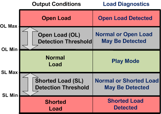
TAS5411-Q1 ld-dia-thr_SLOS814.gifFigure 12. Load Diagnostic Reporting Thresholds