SLLS977F April 2009 – July 2017 SN75DP139
PRODUCTION DATA.
- 1 Features
- 2 Applications
- 3 Description
- 4 Revision History
- 5 Pin Configuration and Functions
-
6 Specifications
- 6.1 Absolute Maximum Ratings
- 6.2 ESD Ratings
- 6.3 Recommended Operating Conditions
- 6.4 Thermal Information
- 6.5 Electrical Characteristics (Device Power)
- 6.6 Electrical Characteristics (Hot Plug Detect)
- 6.7 Electrical Characteristics (Aux / I2C Pins)
- 6.8 Electrical Characteristics (TMDS and Main Link Pins)
- 6.9 Switching Characteristics (Hot Plug Detect)
- 6.10 Switching Characteristics (Aux / I2C Pins)
- 6.11 Switching Characteristics (TMDS and Main Link Pins)
- 6.12 Typical Characteristics
- 7 Detailed Description
- 8 Application and Implementation
- 9 Power Supply Recommendations
- 10Layout
- 11Device and Documentation Support
- 12Mechanical, Packaging, and Orderable Information
封装选项
机械数据 (封装 | 引脚)
散热焊盘机械数据 (封装 | 引脚)
订购信息
1 Features
- DisplayPort Physical Layer Input Port to TMDS Physical Layer Output Port
- Integrated TMDS Level-Shifting Re-driver With Receiver Equalization
- Supports Data Rates up to 3.4 Gbps
- Achieves HDMI 1.4b Compliance
- 3D HDMI Support With TMDS Clock Rates up to 340 MHz
- 4k × 2k Operation (30 Hz, 24bpp)
- Deep Color Supporting 36bpp
- Integrated I2C Logic Block for DVI/HDMI Connector Recognition
- Integrated Active I2C Buffer
- Enhanced ESD: 10 kV on All Pins
- Enhanced Commercial Temperature Range: 0°C to 85°C
- 48-Pin 7-mm × 7-mm VQFN (RGZ) Package
- 40-Pin 5-mm × 5-mm WQFN (RSB) Package
2 Applications
- Personal Computer Market
- DP/TMDS Dongle
- Desktop PC
- Notebook PC
- Docking Station
- Stand-Alone Video Card
3 Description
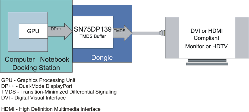
The SN75DP139 is a dual-mode DisplayPort input to Transition-Minimized Differential Signaling (TMDS) output. The TMDS output has a built-in level-shifting re-driver supporting Digital Video Interface (DVI) 1.0 and High Definition Multimedia Interface (HDMI) 1.4b standards. The SN75DP139 is specified up to a maximum data rate of 3.4 Gbps, supporting resolutions greater then 1920 × 1200 or HDTV 12-bit color depth at 1080p (progressive scan). The SN75DP139 is compliant with the HDMI 1.4b specifications and supports optional protocol enhancements such as 3D graphics at resolutions demanding a pixel rate up to 340 MHz.
Device Information(1)
| PART NUMBER | PACKAGE | BODY SIZE (NOM) |
|---|---|---|
| SN75DP139 | VQFN (48) | 7.00 mm x 7.00 mm |
| WQFN (40) | 5.00 mm x 5.00 mm |
- For all available packages, see the orderable addendum at the end of the datasheet.
Typical Application
