ZHCSPK8A December 2021 – August 2022 REF35
PRODUCTION DATA
- 1 特性
- 2 应用
- 3 说明
- 4 Revision History
- 5 Device Comparison
- 6 Pin Configuration and Functions
- 7 Specifications
- 8 Parameter Measurement Information
- 9 Detailed Description
- 10Application and Implementation
- 11Device and Documentation Support
- 12Mechanical, Packaging, and Orderable Information
8.4 Thermal Hysteresis
Thermal hysteresis is measured with the REF35 soldered to a PCB, similar to a real-world application. Thermal hysteresis for the device is defined as the change in output voltage after operating the device at 25°C, cycling the device through the specified temperature range, and returning to 25°C. The PCB was baked at 150°C for 30 minutes before thermal hysteresis was measured. Use Equation 2 to calculate the thermal hysteresis:
Equation 2. 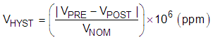
where
- VHYST = thermal hysteresis (in units of ppm)
- VNOM = the specified output voltage
- VPRE = output voltage measured at 25°C pre-temperature cycling
- VPOST = output voltage measured after the device has cycled from 25°C through the specified temperature range of –40°C to +85°C or –40°C to +105°C and returns to 25°C.
The graphs below show the typical thermal hysteresis distribution across various temperature ranges in two cycles.
Figure 8-6 Thermal Hysteresis Distribution
–40ºC to 85ºC, Cycle 1
–40ºC to 85ºC, Cycle 1
Figure 8-8 Thermal Hysteresis
Distribution
–40ºC to 105ºC, Cycle 1
–40ºC to 105ºC, Cycle 1
Figure 8-7 Thermal Hysteresis
Distribution
–40ºC to 85ºC, Cycle 2
–40ºC to 85ºC, Cycle 2
Figure 8-9 Thermal Hysteresis
Distribution
–40ºC to 105ºC, Cycle 2
–40ºC to 105ºC, Cycle 2