ZHCSAC2C August   2012  – October 2018 PCM5121 , PCM5122

PRODUCTION DATA.  

  1. 特性
  2. 应用
  3. 说明
    1.     Device Images
      1.      简化系统图
  4. 修订历史记录
  5. Device Comparison
  6. Pin Configuration and Functions
    1. 6.0.1 RHB Package I2C Mode (MODE1 tied to DGND and MODE2 tied to DVDD) Top View
    2. 6.0.2 RHB Package SPI Mode (MODE1 tied to DVDD) Top View
    3. 6.0.3 RHB Package Hardwired Mode (MODE1 tied to DGND, MODE2 tied to DGND) Top View
    4.     Pin Functions
  7. Specifications
    1. 7.1 Absolute Maximum Ratings
    2. 7.2 ESD Ratings
    3. 7.3 Recommended Operating Conditions
    4. 7.4 Thermal Information
    5. 7.5 Electrical Characteristics
    6. 7.6 Timing Requirements: SCK Input
    7. 7.7 Timing Requirements: XSMT
    8. 7.8 Switching Characteristics
    9. 7.9 Typical Characteristics
  8. Detailed Description
    1. 8.1 Overview
    2. 8.2 Functional Block Diagram
    3. 8.3 Feature Description
      1. 8.3.1 Terminology
      2. 8.3.2 Audio Data Interface
        1. 8.3.2.1 Audio Serial Interface
        2. 8.3.2.2 PCM Audio Data Formats
        3. 8.3.2.3 Zero Data Detect
      3. 8.3.3 XSMT Pin (Soft Mute / Soft Un-Mute)
      4. 8.3.4 Audio Processing
        1. 8.3.4.1 PCM512x Audio Processing
          1. 8.3.4.1.1 Overview
          2. 8.3.4.1.2 Software
        2. 8.3.4.2 Interpolation Filter
        3. 8.3.4.3 Fixed Audio Processing Flow (Program 5)
          1. 8.3.4.3.1 Filter Programming Changes
          2. 8.3.4.3.2 Processing Blocks – Detailed Descriptions
          3. 8.3.4.3.3 Biquad Section
          4. 8.3.4.3.4 Dynamic Range Compression
          5. 8.3.4.3.5 Stereo Mixer
          6. 8.3.4.3.6 Stereo Multiplexer
          7. 8.3.4.3.7 Mono Mixer
          8. 8.3.4.3.8 Master Volume Control
          9. 8.3.4.3.9 Miscellaneous Coefficients
      5. 8.3.5 DAC Outputs
        1. 8.3.5.1 Analog Outputs
        2. 8.3.5.2 Recommended Output Filter for the PCM512x
        3. 8.3.5.3 Choosing Between VREF and VCOM Modes
          1. 8.3.5.3.1 Voltage Reference and Output Levels
          2. 8.3.5.3.2 Mode Switching Sequence, from VREF Mode to VCOM Mode
        4. 8.3.5.4 Digital Volume Control
          1. 8.3.5.4.1 Emergency Ramp-Down
        5. 8.3.5.5 Analog Gain Control
      6. 8.3.6 Reset and System Clock Functions
        1. 8.3.6.1 Clocking Overview
        2. 8.3.6.2 Clock Slave Mode With Master and System Clock (SCK) Input (4 Wire I2S)
        3. 8.3.6.3 Clock Slave Mode With BCK PLL to Generate Internal Clocks (3-Wire PCM)
        4. 8.3.6.4 Clock Generation Using the PLL
        5. 8.3.6.5 PLL Calculation
          1. 8.3.6.5.1 Examples:
            1. 8.3.6.5.1.1 Recommended PLL Settings
        6. 8.3.6.6 Clock Master Mode from Audio Rate Master Clock
        7. 8.3.6.7 Clock Master from a Non-Audio Rate Master Clock
    4. 8.4 Device Functional Modes
      1. 8.4.1 Choosing a Control Mode
        1. 8.4.1.1 Software Control
          1. 8.4.1.1.1 SPI Interface
            1. 8.4.1.1.1.1 Register Read and Write Operation
          2. 8.4.1.1.2 I2C Interface
            1. 8.4.1.1.2.1 Slave Address
            2. 8.4.1.1.2.2 Register Address Auto-Increment Mode
            3. 8.4.1.1.2.3 Packet Protocol
            4. 8.4.1.1.2.4 Write Register
            5. 8.4.1.1.2.5 Read Register
            6. 8.4.1.1.2.6 Timing Characteristics
      2. 8.4.2 VREF and VCOM Modes
    5. 8.5 Programming
  9. Application and Implementation
    1. 9.1 Application Information
    2. 9.2 Typical Application
      1. 9.2.1 Design Requirements
      2. 9.2.2 Detailed Design Procedure
      3. 9.2.3 Application Curve
  10. 10Power Supply Recommendations
    1. 10.1 Power Supply Distribution and Requirements
    2. 10.2 Recommended Powerdown Sequence
      1. 10.2.1 XSMT = 0
      2. 10.2.2 Clock Error Detect
      3. 10.2.3 Planned Shutdown
      4. 10.2.4 Unplanned Shutdown
    3. 10.3 External Power Sense Undervoltage Protection Mode
    4. 10.4 Power-On Reset Function
      1. 10.4.1 Power-On Reset, DVDD 3.3-V Supply
      2. 10.4.2 Power-On Reset, DVDD 1.8-V Supply
    5. 10.5 PCM512x Power Modes
      1. 10.5.1 Setting Digital Power Supplies and I/O Voltage Rails
      2. 10.5.2 Power Save Modes
      3. 10.5.3 Power Save Parameter Programming
  11. 11Layout
    1. 11.1 Layout Guidelines
    2. 11.2 Layout Example
  12. 12Register Maps
    1. 12.1 PCM512x Register Map
      1. 12.1.1 Detailed Register Descriptions
        1. 12.1.1.1 Register Map Summary
        2. 12.1.1.2 Page 0 Registers
        3. 12.1.1.3 Page 1 Registers
        4. 12.1.1.4 Page 44 Registers
        5. 12.1.1.5 Page 253 Registers
      2. 12.1.2 PLL Tables for Software Controlled Devices
      3. 12.1.3 Coefficient Data Formats
      4. 12.1.4 Power Down and Reset Behavior
  13. 13器件和文档支持
    1. 13.1 开发支持
    2. 13.2 文档支持
    3. 13.3 相关链接
    4. 13.4 接收文档更新通知
    5. 13.5 社区资源
    6. 13.6 商标
    7. 13.7 静电放电警告
    8. 13.8 术语表
  14. 14机械、封装和可订购信息

封装选项

机械数据 (封装 | 引脚)
散热焊盘机械数据 (封装 | 引脚)
订购信息

Register Read and Write Operation

All read/write operations for the serial control port use 16-bit data words. Figure 66 shows the control data word format. The most significant bit is the read/write bit. For write operations, the bit must be set to 0. For read operations, the bit must be set to 1. There are seven bits, labeled IDX[6:0], that hold the register index (or address) for the read and write operations. The least significant eight bits, D[7:0], contain the data to be written to, or the data that was read from, the register specified by IDX[6:0].

Figure 66 and Figure 67 show the functional timing diagram to write or read through the serial control port. MS is held at a logic-1 state until a register access. To start the register write or read cycle, set MS to logic 0. Sixteen clocks are then provided on MC, corresponding to the 16 bits of the control data word on MOSI and read-back data on MISO. After the eighth clock cycle has completed, the data from the indexed-mode control register appears on MISO during the read operation. After the sixteenth clock cycle has completed, the data is latched into the indexed-mode control register during the write operation. To write or read subsequent data, MS is set to logic 1 once (see tMHH in Figure 71).

PCM5121 PCM5122 f_pcm51xx_mdi_ctrl_data_word_format.gifFigure 66. Control Data Word Format; MDI

NOTE

B8 is used for selection of Write or Read. Setting = 0 indicates a Write, while = 1 indicates a Read. Bits 15–9 are used for register address. Bits 7–0 are used for register data. Multiple-byte write or read (up to 8 bytes) is supported while MS is kept low. The address field becomes the initial address, automatically incrementing for each byte.

PCM5121 PCM5122 f_pcm51xx_td_ser_ctrl_format_wr.gifFigure 67. Serial Control Format; Write, Single Byte
PCM5121 PCM5122 f_pcm51xx_td_ser_ctrl_format__burst_wr.gifFigure 68. Serial Control Format; Write, Multiple Byte
PCM5121 PCM5122 f_pcm51xx_td_ser_ctrl_format_rd.gifFigure 69. Serial Control Format; Read
PCM5121 PCM5122 f_pcm51xx_td_ser_ctrl_format__burst_rd.gifFigure 70. Serial Control Format; Read, Multiple Byte
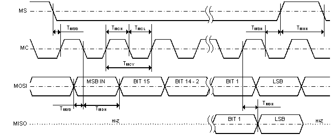
PCM5121 PCM5122 f_pcm51xx_td_ctrl_if.gifFigure 71. Control Interface Timing

Table 37. Control Interface Timing

MIN MAX UNIT
tMCY MC Pulse Cycle Time 100 ns
tMCL MC Low Level Time 40 ns
tMCH MC High Level Time 40 ns
tMHH MS High Level Time 20 ns
tMSS MS ↓ Edge to MC ↑ Edge 30 ns
tMSH MS Hold Time(1) 30 ns
tMDH MDI Hold Time 15 ns
tMDS MDI Set-up Time 15 ns
tMOS MC Rise Edge to MDO Stable 20 ns
MC falling edge for LSB to MS rising edge.