ZHCSAC2C August 2012 – October 2018 PCM5121 , PCM5122
PRODUCTION DATA.
- 1 特性
- 2 应用
- 3 说明
- 4 修订历史记录
- 5 Device Comparison
- 6 Pin Configuration and Functions
- 7 Specifications
-
8 Detailed Description
- 8.1 Overview
- 8.2 Functional Block Diagram
- 8.3
Feature Description
- 8.3.1 Terminology
- 8.3.2 Audio Data Interface
- 8.3.3 XSMT Pin (Soft Mute / Soft Un-Mute)
- 8.3.4 Audio Processing
- 8.3.5 DAC Outputs
- 8.3.6
Reset and System Clock Functions
- 8.3.6.1 Clocking Overview
- 8.3.6.2 Clock Slave Mode With Master and System Clock (SCK) Input (4 Wire I2S)
- 8.3.6.3 Clock Slave Mode With BCK PLL to Generate Internal Clocks (3-Wire PCM)
- 8.3.6.4 Clock Generation Using the PLL
- 8.3.6.5 PLL Calculation
- 8.3.6.6 Clock Master Mode from Audio Rate Master Clock
- 8.3.6.7 Clock Master from a Non-Audio Rate Master Clock
- 8.4 Device Functional Modes
- 8.5 Programming
- 9 Application and Implementation
- 10Power Supply Recommendations
- 11Layout
- 12Register Maps
- 13器件和文档支持
- 14机械、封装和可订购信息
8.3.4.2 Interpolation Filter
The PCM512x provides 4 types of interpolation filters, selectable by writing to Page 0, Register 43, D(4:0).
Table 7. ROM Preset Programs
| PROGRAM NUMBER | D(4:0) | DESCRIPTION | MINIMUM CYCLES |
|---|---|---|---|
| 0 | 0 0000 | Reserved | |
| 1 | 0 0001 | Normal x8/x4/x2/x1 Interpolation Filter(1) | 256 |
| 2 | 0 0010 | Low Latency x8/x4/x2/x1 Interpolation Filter(1) | 256 |
| 3 | 0 0011 | High Attenuation x8/x4/x2 Interpolation Filter(1) | 512 |
| 4 | 0 0100 | Reserved | |
| 5 | 0 0101 | Preset Process Flow | |
| 6 | 0 0110 | Reserved | |
| 7 | 0 0111 | Asymmetric FIR Interpolation Filter(1) | 512 |
| : | : | Reserved | |
| 31 | 1 1111 | Reserved |
(1) At fs=44.1 kHz, de-emphasis filter is supported.
The PCM512x supports four sampling modes (single rate, dual rate, quad rate, and octal rate) which produce different oversampling rates (OSR) in the interpolation digital filter operation. These are shown in Table 8.
Table 8. Sampling Modes and Oversampling Rates
| SAMPLING MODE | SAMPLING FREQUENCY (fS) kHz | OVERSAMPLING RATE (OSR) |
|---|---|---|
| Single Rate | 8 | 8 or 16 |
| 16 | ||
| 32 | ||
| 44.1 | ||
| 48 | ||
| Dual Rate | 88.2 | 4 |
| 96 | ||
| Quad Rate | 176.4 | 2 |
| 192 | ||
| Octal Rate | 384 | 1 (Bypass) |
Table 9. Normal x8 Interpolation Filter, Single Rate
| PARAMETER | CONDITION | VALUE (TYP) | VALUE (MAX) | UNIT |
|---|---|---|---|---|
| Filter Gain Pass Band | 0 ……. 0.45 × fS | dB | ||
| Filter Gain Stop Band | 0.55 × fS ….. 7.455 × fS | dB | ||
| Filter Group Delay | 20 / fs | S |
SPACE
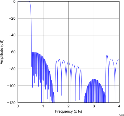 Figure 19. Normal x8 Interpolation Filter
Frequency Response
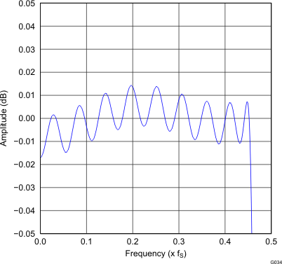 Figure 21. Normal x8 Interpolation Filter Passband Ripple
 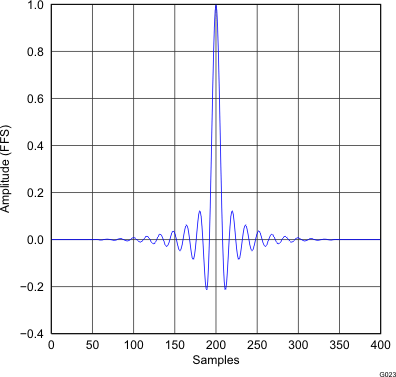 Figure 20. Normal x8 Interpolation Filter
Impulse Response
Table 10. Normal x4 Interpolation Filter, Dual Rate
| PARAMETER | CONDITION | VALUE (TYP) | VALUE (MAX) | UNIT |
|---|---|---|---|---|
| Filter Gain Pass Band | 0 ……. 0.45 × fS | dB | ||
| Filter Gain Stop Band | 0.55 × fS ….. 3.455 × fS | dB | ||
| Filter Group Delay | 20 / fs | S |
SPACE
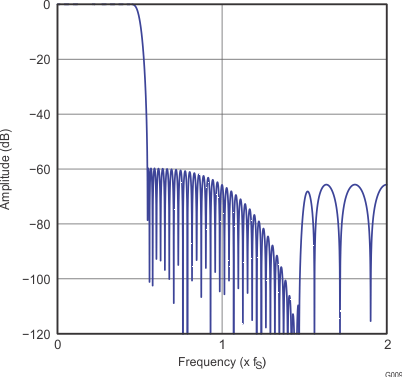 Figure 22. Normal x4 Interpolation Filter
Frequency Response
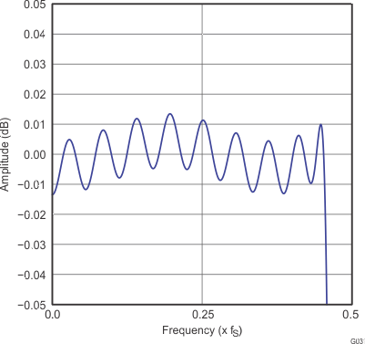 Figure 24. Normal x4 Interpolation Filter Passband Ripple
 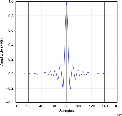 Figure 23. Normal x4 Interpolation Filter
Impulse Response
Table 11. Normal x2 Interpolation Filter, Quad Rate
| PARAMETER | CONDITION | VALUE (TYP) | VALUE (MAX) | UNIT |
|---|---|---|---|---|
| Filter Gain Pass Band | 0 ……. 0.45 × fS | dB | ||
| Filter Gain Stop Band | 0.55 × fS ….. 1.455 × fS | dB | ||
| Filter Group Delay | 20 / fs | S |
SPACE
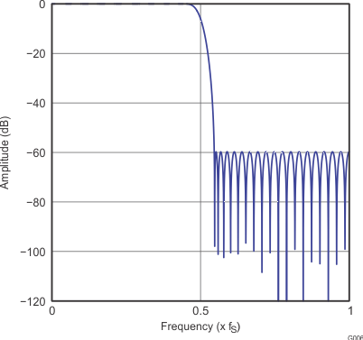 Figure 25. Normal x2 Interpolation Filter
Frequency Response
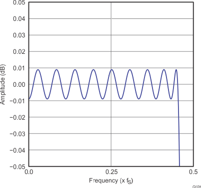 Figure 27. Normal x2 Interpolation Filter Passband Ripple
 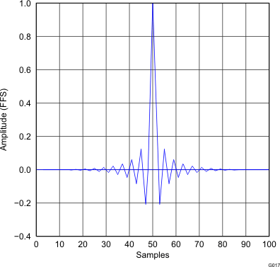 Figure 26. Normal x2 Interpolation Filter
Impulse Response
Table 12. Low Latency x8 Interpolation Filter, Single Rate
| PARAMETER | CONDITION | VALUE (TYP) | VALUE (MAX) | UNIT |
|---|---|---|---|---|
| Filter Gain Pass Band | 0 ……. 0.45 × fS | dB | ||
| Filter Gain Stop Band | 0.55 × fS ….. 7.455 × fS | dB | ||
| Filter Group Delay | S |
SPACE
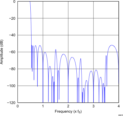 Figure 28. Low Latency x8 Interpolation Filter
Frequency Response
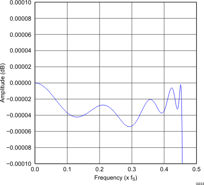 Figure 30. Low Latency x8 Interpolation Filter Passband Ripple
 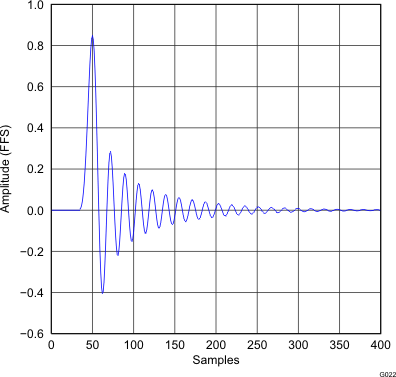 Figure 29. Low Latency x8 Interpolation Filter
Impulse Response
Table 13. Low Latency x4 Interpolation Filter, Dual Rate
| PARAMETER | CONDITION | VALUE (TYP) | VALUE (MAX) | UNIT |
|---|---|---|---|---|
| Filter Gain Pass Band | 0 ……. 0.45 × fS | dB | ||
| Filter Gain Stop Band | 0.55 × fS ….. 3.455 × fS | dB | ||
| Filter Group Delay | S |
SPACE
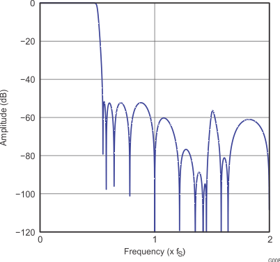 Figure 31. Low Latency x4 Interpolation Filter
Frequency Response
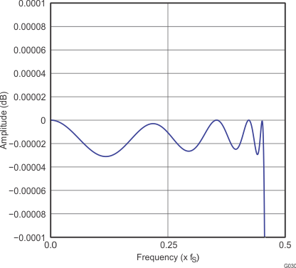 Figure 33. Low Latency x4 Interpolation Filter Passband Ripple
 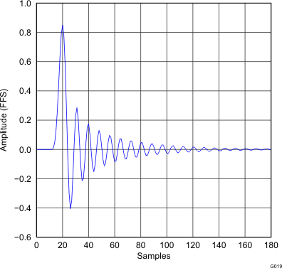 Figure 32. Low Latency x4 Interpolation Filter
Impulse Response
Table 14. Low Latency ×2 Interpolation Filter, Quad Rate
| PARAMETER | CONDITION | VALUE (TYP) | VALUE (MAX) | UNIT |
|---|---|---|---|---|
| Filter Gain Pass Band | 0 ……. 0.45 × fS | dB | ||
| Filter Gain Stop Band | 0.55 × fS ….. 1.455 × fS | dB | ||
| Filter Group Delay | S |
SPACE
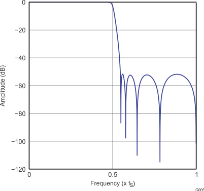 Figure 34. Low Latency x2 Interpolation Filter
Frequency Response
 Figure 36. Low Latency x2 Interpolation Filter Passband Ripple
 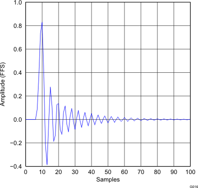 Figure 35. Low Latency x2 Interpolation Filter
Impulse Response
Table 15. Asymmetric FIR x8 Interpolation Filter, Single Rate
| PARAMETER | CONDITION | VALUE (TYP) | VALUE (MAX) | UNIT |
|---|---|---|---|---|
| Filter Gain Pass Band | 0 ……. 0.40 × fS | ±0.05 | dB | |
| Filter Gain Stop Band | 0.72 × fS ….. 7.28 × fS | –50 | dB | |
| Filter Group Delay | 1.2 × ts | S |
SPACE
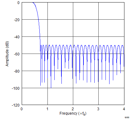 Figure 37. Asymmetric FIR x8 Interpolation Filter Frequency Response, Single Rate
 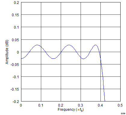 Figure 39. Asymmetric FIR x8 Interpolation Filter Passband Ripple, Single Rate
 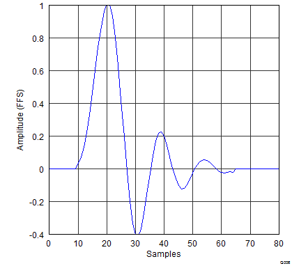 Figure 38. Asymmetric FIR x8 Interpolation Filter Impulse Response, Single Rate
 Table 16. Asymmetric FIR x4 Interpolation Filter, Dual Rate
| PARAMETER | CONDITION | VALUE (TYP) | VALUE (MAX) | UNIT |
|---|---|---|---|---|
| Filter Gain Pass Band | 0 ……. 0.40 × fS | ±0.05 | dB | |
| Filter Gain Stop Band | 0.72 × fS ….. 3.28 × fS | –50 | dB | |
| Filter Group Delay | 1.2 × ts | S |
SPACE
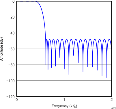 Figure 40. Asymmetric FIR x4 Interpolation Filter Frequency Response, Dual Rate
 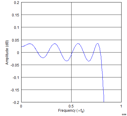 Figure 42. Asymmetric x4 Interpolation Filter Passband Ripple, Dual Rate
 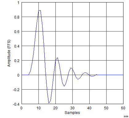 Figure 41. Asymmetric FIR x4 Interpolation Filter Impulse Response, Dual Rate
 Table 17. Asymmetric FIR x2 Interpolation Filter, Quad Rate
| PARAMETER | CONDITION | VALUE (TYP) | VALUE (MAX) | UNIT |
|---|---|---|---|---|
| Filter Gain Pass Band | 0 ……. 0.40 × fS | ±0.05 | dB | |
| Filter Gain Stop Band | 0.72 × fS ….. 1.28 × fS | –50 | dB | |
| Filter Group Delay | 1.2 × ts | S |
SPACE
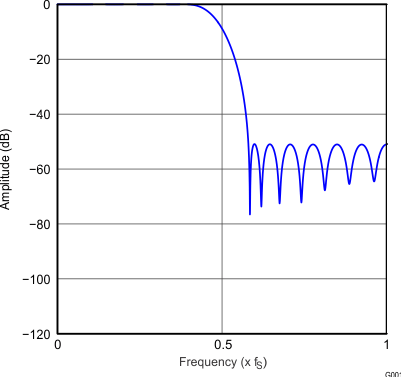 Figure 43. Asymmetric FIR x2 Interpolation Filter Frequency Response, Quad Rate
 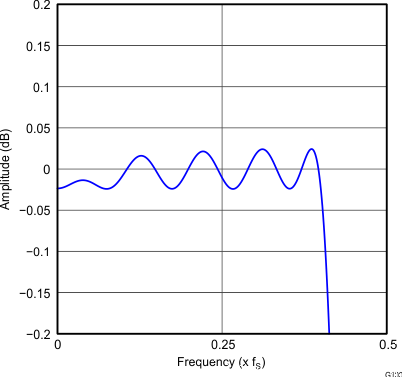 Figure 45. Asymmetric x2 Interpolation Filter Passband Ripple, Quad Rate
 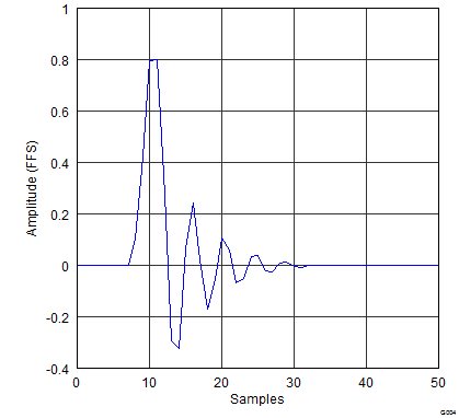 Figure 44. Asymmetric FIR x2 Interpolation Filter Impulse Response, Quad Rate
 Table 18. High-Attentuation x8 Interpolation Filter, Single Rate
| PARAMETER | CONDITION | VALUE (TYP) | VALUE (MAX) | UNIT |
|---|---|---|---|---|
| Filter Gain Pass Band | 0 ……. 0.45 × fS | ±0.0005 | dB | |
| Filter Gain Stop Band | 0.55 × fS ….. 7.455 × fS | –100 | dB | |
| Filter Group Delay | 33.7 × tS | S |
SPACE
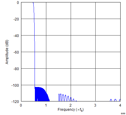 Figure 46. High-Attentuation x8 Interpolation Filter Frequency Response, Single Rate
 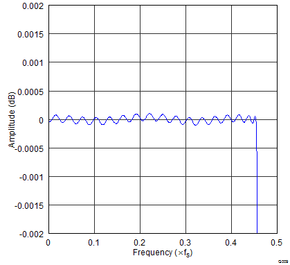 Figure 48. High-Attentuation x8 Interpolation Filter Passband Ripple, Single Rate
 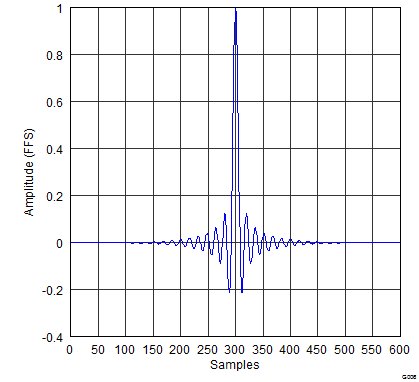 Figure 47. High-Attentuation x8 Interpolation Filter Impulse Response, Single Rate
 Table 19. High-Attentuation x4 Interpolation Filter, Dual Rate
| PARAMETER | CONDITION | VALUE (TYP) | VALUE (MAX) | UNIT |
|---|---|---|---|---|
| Filter Gain Pass Band | 0 ……. 0.45 × fS | ±0.0005 | dB | |
| Filter Gain Stop Band | 0.55 × fS ….. 3.455 × fS | –100 | dB | |
| Filter Group Delay | 33.7 × tS | S |
SPACE
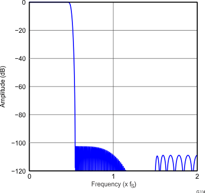 Figure 49. High-Attentuation x4 Interpolation Filter Frequency Response, Dual Rate
 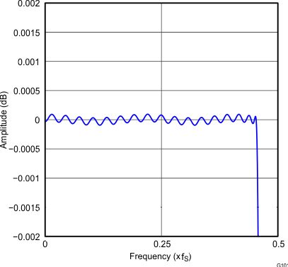 Figure 51. High-Attentuation x4 Interpolation Filter Passband Ripple, Dual Rate
 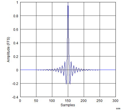 Figure 50. High-Attentuation x4 Interpolation Filter Impulse Response, Dual Rate
 Table 20. High-Attentuation x2 Interpolation Filter, Quad Rate
| PARAMETER | CONDITION | VALUE (TYP) | VALUE (MAX) | UNIT |
|---|---|---|---|---|
| Filter Gain Pass Band | 0 ……. 0.45 × fS | ±0.0005 | dB | |
| Filter Gain Stop Band | 0.55 × fS ….. 1.455 × fS | –100 | dB | |
| Filter Group Delay | 33.7 × tS | S |
SPACE
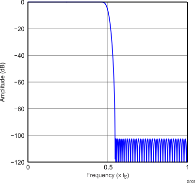 Figure 52. High-Attentuation x2 Interpolation Filter Frequency Response, Quad Rate
 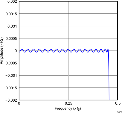 Figure 54. High-Attentuation x2 Interpolation Filter Passband Ripple, Quad Rate
 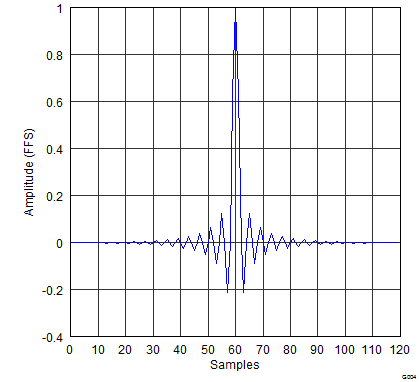 Figure 53. High-Attentuation x2 Interpolation Filter Impulse Response, Quad Rate