ZHCSGP3D September 2017 – December 2018 OPA2837 , OPA837
PRODUCTION DATA.
- 1 特性
- 2 应用
- 3 说明
- 4 修订历史记录
- 5 Pin Configuration and Functions
-
6 Specifications
- 6.1 Absolute Maximum Ratings
- 6.2 ESD Ratings
- 6.3 Recommended Operating Conditions
- 6.4 Thermal Information: OPA837
- 6.5 Thermal Information: OPA2837
- 6.6 Electrical Characteristics: VS = 5 V
- 6.7 Electrical Characteristics: VS = 3 V
- 6.8 Typical Characteristics: VS = 5.0 V
- 6.9 Typical Characteristics: VS = 3.0 V
- 6.10 Typical Characteristics: ±2.5-V to ±1.5-V Split Supply
- 7 Detailed Description
-
8 Application and Implementation
- 8.1
Application Information
- 8.1.1 Noninverting Amplifier
- 8.1.2 Inverting Amplifier
- 8.1.3 Output DC Error Calculations
- 8.1.4 Output Noise Calculations
- 8.1.5 Instrumentation Amplifier
- 8.1.6 Attenuators
- 8.1.7 Differential to Single-Ended Amplifier
- 8.1.8 Differential-to-Differential Amplifier
- 8.1.9 Pulse Application With Single-Supply Circuit
- 8.1.10 ADC Driver Performance
- 8.2 Typical Applications
- 8.1
Application Information
- 9 Power Supply Recommendations
- 10Layout
- 11器件和文档支持
- 12机械、封装和可订购信息
5 Pin Configuration and Functions
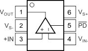
OPA837 DBV Package
6-Pin SOT-23
Top View

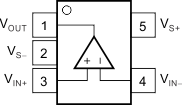
OPA837 DCK Package
5-Pin SC70
Top View

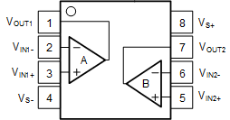
OPA2837 DGK Package
8-Pin VSSOP
Top View

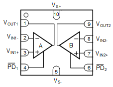
OPA2837 RUN Package
10-Pin WQFN
Top View

Pin Functions
| PIN | FUNCTION(1) | DESCRIPTION | ||||
|---|---|---|---|---|---|---|
| NAME | OPA837 | OPA2837 | ||||
| SOT-23 | SC-70 | VSSOP | WQFN | |||
| PD | 5 | — | — | — | I | Amplifier power down.
Low = disabled, high = normal operation (pin must be driven). |
| PD1 | — | — | — | 4 | I | Amplifier 1 power down.
Low = disabled, high = normal operation (pin must be driven). |
| PD2 | — | — | — | 6 | I | Amplifier 2 power down.
Low = disabled, high = normal operation (pin must be driven). |
| VIN– | 4 | 4 | — | — | I | Inverting input pin |
| VIN+ | 3 | 3 | — | — | I | Noninverting input pin |
| VIN1– | — | — | 2 | 2 | I | Amplifier 1 inverting input pin |
| VIN1+ | — | — | 3 | 3 | I | Amplifier 1 noninverting input pin |
| VIN2– | — | — | 6 | 8 | I | Amplifier 2 inverting input pin |
| VIN2+ | — | — | 5 | 7 | I | Amplifier 2 noninverting input pin |
| VOUT | 1 | 1 | — | — | O | Output pin |
| VOUT1 | — | — | 1 | 1 | O | Amplifier 1 output pin |
| VOUT2 | — | — | 7 | 9 | O | Amplifier 2 output pin |
| VS– | 2 | 2 | 4 | 5 | P | Negative power-supply pin |
| VS+ | 6 | 5 | 8 | 10 | P | Positive power-supply input |
(1) I = input, O = output, and P = power.