ZHCSGP3D September   2017  – December 2018 OPA2837 , OPA837

PRODUCTION DATA.  

  1. 特性
  2. 应用
    1.     具有真正接地输入和输出范围的低功耗、低噪声、精密单端 SAR ADC 驱动器
  3. 说明
    1.     Device Images
  4. 修订历史记录
  5. Pin Configuration and Functions
    1.     Pin Functions
  6. Specifications
    1. 6.1  Absolute Maximum Ratings
    2. 6.2  ESD Ratings
    3. 6.3  Recommended Operating Conditions
    4. 6.4  Thermal Information: OPA837
    5. 6.5  Thermal Information: OPA2837
    6. 6.6  Electrical Characteristics: VS = 5 V
    7. 6.7  Electrical Characteristics: VS = 3 V
    8. 6.8  Typical Characteristics: VS = 5.0 V
    9. 6.9  Typical Characteristics: VS = 3.0 V
    10. 6.10 Typical Characteristics: ±2.5-V to ±1.5-V Split Supply
  7. Detailed Description
    1. 7.1 Overview
    2. 7.2 Functional Block Diagrams
    3. 7.3 Feature Description
      1. 7.3.1 OPA837 Comparison
      2. 7.3.2 Input Common-Mode Voltage Range
      3. 7.3.3 Output Voltage Range
      4. 7.3.4 Power-Down Operation
      5. 7.3.5 Low-Power Applications and the Effects of Resistor Values on Bandwidth
      6. 7.3.6 Driving Capacitive Loads
    4. 7.4 Device Functional Modes
      1. 7.4.1 Split-Supply Operation (±1.35 V to ±2.7 V)
      2. 7.4.2 Single-Supply Operation (2.7 V to 5.4 V)
  8. Application and Implementation
    1. 8.1 Application Information
      1. 8.1.1  Noninverting Amplifier
      2. 8.1.2  Inverting Amplifier
      3. 8.1.3  Output DC Error Calculations
      4. 8.1.4  Output Noise Calculations
      5. 8.1.5  Instrumentation Amplifier
      6. 8.1.6  Attenuators
      7. 8.1.7  Differential to Single-Ended Amplifier
      8. 8.1.8  Differential-to-Differential Amplifier
      9. 8.1.9  Pulse Application With Single-Supply Circuit
      10. 8.1.10 ADC Driver Performance
    2. 8.2 Typical Applications
      1. 8.2.1 Active Filters
        1. 8.2.1.1 Design Requirements
        2. 8.2.1.2 Detailed Design Procedure
        3. 8.2.1.3 Application Curves
      2. 8.2.2 Implementing a 2:1 Active Multiplexer
        1. 8.2.2.1 Design Requirements
        2. 8.2.2.2 Detailed Design Procedure
      3. 8.2.3 1-Bit PGA Operation
        1. 8.2.3.1 Design Requirements
        2. 8.2.3.2 Detailed Design Procedure
  9. Power Supply Recommendations
  10. 10Layout
    1. 10.1 Layout Guidelines
    2. 10.2 Layout Example
  11. 11器件和文档支持
    1. 11.1 文档支持
      1. 11.1.1 相关文档
    2. 11.2 相关链接
    3. 11.3 接收文档更新通知
    4. 11.4 社区资源
    5. 11.5 商标
    6. 11.6 静电放电警告
    7. 11.7 术语表
  12. 12机械、封装和可订购信息

封装选项

机械数据 (封装 | 引脚)
散热焊盘机械数据 (封装 | 引脚)
订购信息

Typical Characteristics: VS = 5.0 V

at VS+ = 5.0 V, VS– = 0 V, VOUT = 2 VPP, RF = 0 Ω, RL = 2 kΩ, G = 1 V/V, input and output referenced to mid-supply, and TA ≈ 25°C (unless otherwise noted)
OPA837 OPA2837 D001_SBOS673.gif
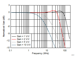
See Figure 74 and Table 2, VOUT = 20 mVPP, RLOAD = 2 kΩ
Figure 1. Noninverting Small-Signal Frequency Response
vs Gain
OPA837 OPA2837 D003_SBOS673.gif
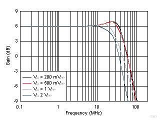
Gain = 2 V/V, RLOAD = 2 kΩ
Figure 3. Noninverting Large-Signal Bandwidth vs VOPP
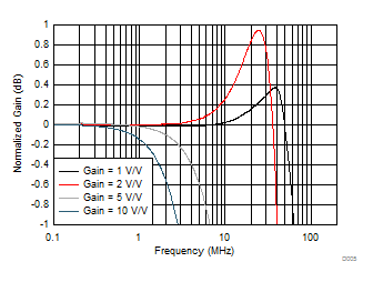
OPA837 OPA2837 D005_SBOS673.gif
See Figure 74 and Table 2, VOUT = 200 mVPP, RLOAD = 2 kΩ
Figure 5. Noninverting Response Flatness vs Gain
OPA837 OPA2837 D007_SBOS673.gif
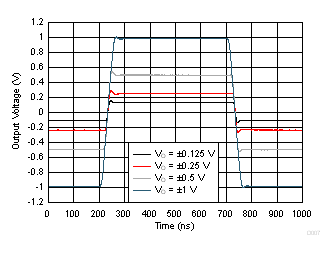
See Figure 74, gain = 2 V/V,
input edge rate set to stay below slew limiting
Figure 7. Noninverting Step Response vs Time and VOPP
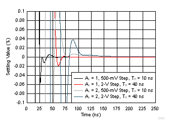
OPA837 OPA2837 D009_SBOS673.gif
See Figure 74 and Table 2
Figure 9. Simulated Noninverting Settling Time
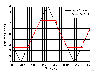
OPA837 OPA2837 D011_SBOS673.gif
See Figure 74 and Table 2, gain = 2 V/V
Figure 11. Noninverting Overdrive Recovery
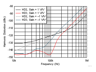
OPA837 OPA2837 D013_SBOS673.gif
See Figure 74, Figure 75, Table 2, and Table 3, VOUT = 2 VPP
Figure 13. Harmonic Distortion vs Frequency
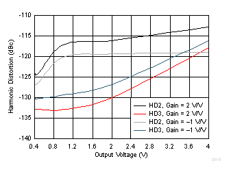
OPA837 OPA2837 D015_SBOS673.gif
See Figure 74, Figure 75, Table 2, and Table 3, VOUT = 2 VPP,
f = 100 kHz
Figure 15. Harmonic Distortion vs Output Voltage
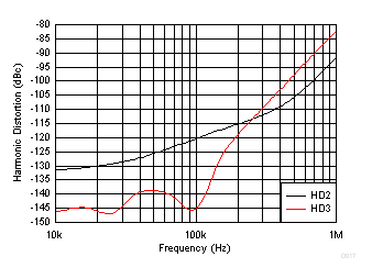
OPA837 OPA2837 D017_SBOS673.gif
See Figure 87, VOUT = 2 VPP, f = 100 kHz
Figure 17. Harmonic Distortion as Active Mux
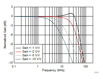
OPA837 OPA2837 D002_SBOS673.gif
See Figure 75 and Table 3, VOUT = 20 mVPP, RLOAD = 2 kΩ
Figure 2. Inverting Small-Signal Frequency Response
vs Gain
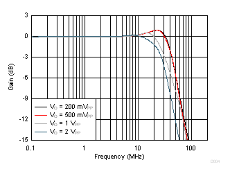
OPA837 OPA2837 D004_SBOS673.gif
Gain = –1 V/V, RLOAD = 2 kΩ
Figure 4. Inverting Large-Signal Bandwidth vs VOPP
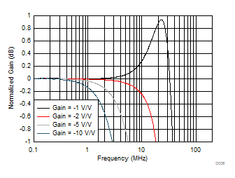
OPA837 OPA2837 D006_SBOS673.gif
See Figure 75 and Table 3, VOUT = 200 mVPP, RLOAD = 2 kΩ
Figure 6. Inverting Response Flatness vs Gain
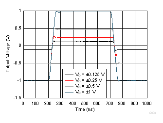
OPA837 OPA2837 D008_SBOS673.gif
See Figure 75, gain = –1 V/V,
input edge rate set to stay below slew limiting
Figure 8. Inverting Step Response vs Time and VOPP
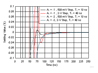
OPA837 OPA2837 D010_SBOS673.gif
See Figure 75 and Table 3
Figure 10. Simulated Inverting Settling Time
OPA837 OPA2837 D012_SBOS673.gif
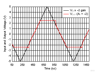
See Figure 75 and Table 3, gain –2 V/V
Figure 12. Inverting Overdrive Recovery
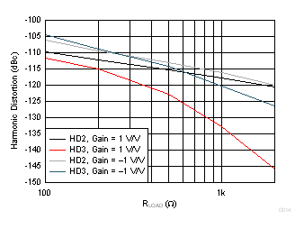
OPA837 OPA2837 D014_SBOS673.gif
See Figure 74, Figure 75, Table 2, and Table 3, VOUT = 2 VPP,
f = 100 kHz
Figure 14. Harmonic Distortion vs RLOAD
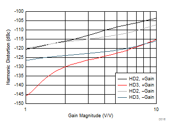
OPA837 OPA2837 D016_SBOS673.gif
See Figure 74, Figure 75, Table 2, and Table 3, VOUT = 2 VPP,
f = 100 kHz
Figure 16. Harmonic Distortion vs Gain Magnitude
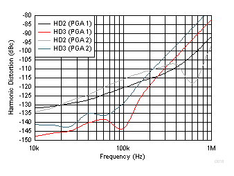
OPA837 OPA2837 D018_SBOS673.gif
See Figure 87, gain of 1 V/V or 2 V/V, VOUT = 2 VPP,
f = 100 kHz
Figure 18. Harmonic Distortion as 1-Bit PGA