SBOS293H December 2003 – December 2015 OPA695
PRODUCTION DATA.
- 1 Features
- 2 Applications
- 3 Description
- 4 Revision History
- 5 Pin Configuration and Functions
- 6 Specifications
- 7 Parameter Measurement Information
-
8 Detailed Description
- 8.1 Overview
- 8.2 Functional Block Diagram
- 8.3 Feature Description
- 8.4 Device Functional Modes
- 9 Application and Implementation
- 10Power Supply Recommendations
- 11Layout
- 12Device and Documentation Support
- 13Mechanical, Packaging, and Orderable Information
封装选项
机械数据 (封装 | 引脚)
散热焊盘机械数据 (封装 | 引脚)
- DGK|8
订购信息
8 Detailed Description
8.1 Overview
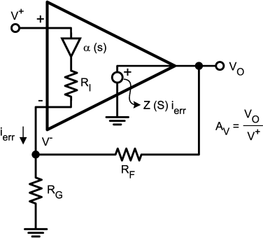
The OPA695, seen below in the Functional Block Diagram, is an operational amplifier with time-proven current feedback architecture. Advantages of current feedback include no gain bandwidth product limitations, fast slew rate, high large signal bandwidth and excellent distortion performance at high frequencies and large amplitudes. Common applications for current feedback operational amplifiers include coaxial cable drivers, ADC drivers, video amplifiers and high frequency gain blocks.
8.2 Functional Block Diagram
8.3 Feature Description
8.3.1 Wideband Current Feedback Operation
The OPA695 provides a new level of performance in wideband current feedback operational amplifiers. Nearly constant AC performance over a wide gain range, along with 4300-V/μs slew rate, gives a lower power and cost solution for high-intercept IF amplifier requirements. While optimized at a gain of +8 V/V (12 dB to a matched 50-Ω load) to give 450-MHz bandwidth, applications from gains of 1 to 40 can be supported. As a gain of +2 video line driver, the bandwidth extends to 1.4 GHz with a slew rate to support the highest pixel rates. At gains above 20, the signal bandwidth starts to decrease, but still exceeds 180 MHz up to a gain of 40 V/V (26 dB to a matched 50-Ω load). Single +5-V supply operation is also supported with similar bandwidths but reduced output power capability. For lower speed (< 250-MHz) requirements with higher output powers, consider the OPA691.
Figure 48 shows the DC-coupled, gain of +8 V/V, dual-power supply circuit used as the basis of the ±5-V Specifications and Typical Characteristic curves. For test purposes, the input impedance is set to 50 Ω with a resistor to ground, and the output impedance is set to 50 Ω with a series output resistor. Voltage swings reported in the specifications are taken directly at the input and output pins, while load powers (dBm) are defined at a matched 50-Ω load. For the circuit of Figure 48, the total effective load is 100 Ω || 458 Ω = 82 Ω. The disable control line (DIS) is typically left open for normal amplifier operation. The disable line must be asserted low to shut off the OPA695. One optional component is included in Figure 48. In addition to the usual power supply decoupling capacitors to ground, a 0.01-μF capacitor is included between the two power supply pins. In practical PCB layouts, this optional added capacitor typically improves the 2nd-harmonic distortion performance by 3 dB to 6 dB for bipolar supply operation.
Figure 49 shows the DC-coupled, gain of –8 V/V, dual-power supply circuit used as the basis of the Inverting Typical Characteristic curves. Inverting operation offers several performance benefits. Because there is no common-mode signal across the input stage, the slew rate for inverting operation is higher and the distortion performance is slightly improved. An additional input resistor, RT, is included in Figure 49 to set the input impedance equal to 50 Ω. The parallel combination of RT and RG set the input impedance. Both the non-inverting and inverting applications of Figure 48 and Figure 49 benefit from optimizing the feedback resistor (RF) value for bandwidth (see the discussion in Setting Resistor Values to Optimize Bandwidth). The typical design sequence is to select the RF value for best bandwidth, set RG for the gain, then set RT for the desired input impedance. As the gain increases for the inverting configuration, a point is reached where RG equals 50 Ω, where RT is removed, and the input match is set by RG only. With RG fixed to achieve an input match to 50 Ω, RF is increased to increase gain. This quickly reduces the achievable bandwidth, as shown by the inverting gain of –16 frequency response in the Typical Characteristic curves. For gains > 10 V/V (14 dB at the matched load), noninverting operation is recommended to maintain broader bandwidth.
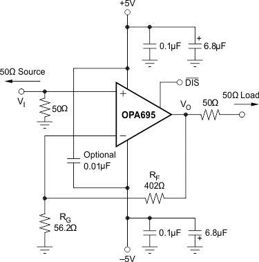 Figure 48. DC-Coupled, G = +8 V/V, Bipolar Supply Specifications and Test Circuit
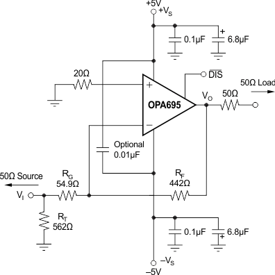 Figure 49. DC-Coupled, G = –8 V/V, Bipolar Supply Specifications and Test Circuit
Figure 50 shows the AC-coupled, single +5-V supply, gain of +8 V/V circuit configuration used as a basis for the +5V-only Specifications and Typical Characteristic curves. The key requirement for broadband single-supply operation is to maintain input and output signal swings within the useable voltage ranges at both the input and the output. The circuit of Figure 50 establishes an input midpoint bias using a simple resistive divider from the +5-V supply (two 806-Ω resistors) to the noninverting input. The input signal is then AC-coupled into this midpoint-voltage bias. The input voltage can swing to within 1.6 V of either supply pin, giving a 1.8-VPP input signal range centered between the supply pins. The input impedance matching resistor (57.6 Ω) used in Figure 50 is adjusted to give a 50-Ω input match when the parallel combination of the biasing divider network is included. The gain resistor (RG) is AC-coupled, giving the circuit a DC gain of +1. This puts the input DC bias voltage (2.5 V) on the output as well. The feedback resistor value has been adjusted from the bipolar supply condition to re-optimize for a flat frequency response in +5 V only, gain of +8 operation (see Setting Resistor Values to Optimize Bandwidth). On a single +5-V supply, the output voltage can swing to within 1.0 V of either supply pin while delivering more than 90-mA output current, giving 3-V output swing into 100 Ω (7-dBm maximum at the matched load). The circuit in Figure 50 shows a blocking capacitor driving into a 50-Ω output resistor, then into a 50-Ω load. Alternatively, the blocking capacitor could be removed with the load tied to a supply midpoint, or to ground if the DC current required by this grounded load is acceptable.
Figure 51 shows the AC-coupled, single +5-V supply, gain of –8 V/V circuit configuration used as a basis for the +5V-only Typical Characteristic curves. In this case, the midpoint DC bias on the noninverting input is also de-coupled with an additional 0.1-μF decoupling capacitor. This reduces the source impedance at higher frequencies for the noninverting input bias current noise. This 2.5-V bias on the noninverting input pin appears on the inverting input pin and, because RG is DC-blocked by the input capacitor, also appears at the output pin. One advantage to inverting operation is that as there is no signal swing across the input stage, higher slew rates and operation to lower supply voltages are possible. To retain a 1-VPP output capability, operation down to a 3-V supply is allowed. At a +3-V supply, the input common mode range is 0 V. However, for the inverting configuration of a current feedback amplifier, wideband operation is retained even with the input stage saturated.
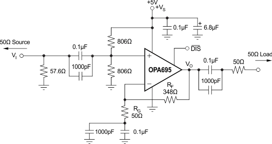 Figure 50. AC-Coupled, G = +8 V/V, Single-Supply Specifications and Test Circuit
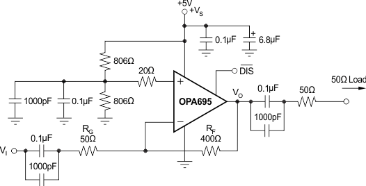 Figure 51. AC-Coupled, G = –8 V/V, Single-Supply Specifications and Test Circuit
The single-supply test circuits of Figure 50 and Figure 51 show +5-V operation. These same circuits can be used over a single-supply range of +5 V to +12 V. Operating on a single +12-V supply, with the Absolute Maximum Supply voltage specification of +13 V, gives adequate design margin for the typical ±5% supply tolerance.
8.3.2 RF Specifications and Applications
The ultra-high, full-power bandwidth and 3rd-order intercept of the OPA695 are ideal for IF amplifier applications. The advantage of a wideband operational amplifier such as the OPA695 include good (and independent) I/O impedance matching, as well as high reverse isolation. A designer accustomed to fixed-gain RF amplifiers will get almost perfect gain accuracy, higher I/O return loss, and 3rd-order intercept points exceeding 30 dBm (up to 110 MHz) using only a 13-mA supply current for the OPA695. Using the considerable design freedom achieved by adjusting the external resistors, the OPA695 can replace a wide range of fixed-gain RF amplifiers with a single part. To understand (in RF amplifier terms) how to take advantage of this, consider first the 4-S parameters (see the example circuits of Figure 48 and Figure 49 on ±5-V supplies, but similar results can be obtained on a single +5-V to +12-V supply).
8.3.3 Input Return Loss (S11)
Input return loss is a measure of how closely (over frequency) the input impedance matches the source impedance. This is relatively independent of gain setting for both the noninverting and inverting configurations. The Typical Characteristics show the magnitude of S11 for the circuits of Figure 48 and Figure 49 through 1 GHz (noninverting gain of +8 and inverting gain of –8 operation, respectively). Noninverting operation offers much better matching to higher frequencies, with the only deviation due to the parasitic input capacitance of the input pin. The noninverting input match is simply set by the resistor to ground on the noninverting input, as the amplifier itself shows a very high input impedance. Inverting operation is also good, but rises more quickly due to loop gain roll-off effects appearing at the inverting node. The inverting mode input match is set by the parallel combination of RG and RT in Figure 49, as the inverting amplifier node may be considered a virtual ground. A good, fixed-gain, RF amplifier would have an input, Voltage Standing Wave Ratio (VSWR) < 1.2:1. This corresponds to an S11 of –21 dB. The OPA695 exceeds this performance through 100 MHz for the inverting mode of operation, and through 400 MHz for the noninverting mode.
8.3.4 Output Return Loss (S22)
Output return loss is a measure of how closely (over frequency) the output impedance matches the load impedance. This is relatively independent of gain setting for both the noninverting and inverting configurations. The output matching impedance, to a first order, is set by adding a series resistor to the low impedance output of the operational amplifier.
Because the operational amplifier itself shows a low output impedance that increases with frequency, an improvement in the output match can therefore be obtained by adding a small equalizing capacitor across this output resistor. The Typical Characteristics show the measured S22 with and without this 2.5-pF capacitor (across the 50-Ω output resistor). Again, a good match for a fixed-gain RF amplifier would give a VSWR of 1.2:1 (S22 < –21 dB). The Typical Characteristic curves show that a simple 50-Ω output resistor holds better than –21 dB to 140 MHz, but up to 380 MHz with the tuning capacitor.
8.3.5 Forward Gain (S21)
In all high-speed amplifier data sheets, forward gain is the small signal gain plotted over frequency. The difference between noninverting and inverting operation is that the phase of S21 starts out at 0° for the noninverting and –180° for the inverting. This initial phase shift for inverting mode is inconsequential to most IF strip applications. The phase of S21 was not shown in Typical Characteristics, but is linear with frequency and may be accurately modeled as a constant time delay through the amplifier.
The Typical Characteristics show S21 over a range of signal gains, where the external resistors have been adjusted to re-optimize flatness at each gain setting. Because this is a current feedback operational amplifier, the signal bandwidth can be held relatively constant as the desired gain setting is changed. The plot of the noninverting bandwidth versus gain shows some change in bandwidth versus gain (due to parasitic capacitive effects on the inverting node) with very little change showing up for the inverting mode of operation.
Signal gains are most often referred to as V/V in operational amplifier data sheets. This is the voltage gain from input to output and is set by external resistor ratios. Because the output impedance is set by a physical series resistor, the voltage gain to the matched load is cut in half by this resistor divider. The log gain to the matched load for the noninverting circuit of Figure 48 is:

The log gain to the matched load for the inverting circuit of Figure 49 is:

The specific resistor values used in Figure 48 and Figure 49 give both a maximally-flat bandwidth and a 12-dB gain to the matched load. The design tables located in the Noise Figure section summarize the required resistor values over a range of desired gains for the circuits of Figure 48 and Figure 49.
As the desired signal gain increases, the achievable bandwidths decrease. In the noninverting case, it decreases relatively quickly as shown in Typical Characteristics. The inverting configuration holds almost constant bandwidth (with correctly selected external resistor values) until RG reduces to equal 50 Ω, and remains at that value to satisfy the input impedance matching requirement, with further increases in gain achieved by increasing RF in Figure 49. The bandwidth then decreases rapidly as shown by the gain of –16 V/V plot in Typical Characteristics.
8.3.6 Reverse Isolation (S12)
Reverse isolation is a measure of how much power injected into the output pin returns to the source. This is rarely specified for an operational amplifier because operational amplifiers are nearly uni-directional signal devices. Below 300 MHz, the noninverting configuration of Figure 48 gives much better isolation than the inverting of Figure 49. Both are well below 40-dB isolation through 350 MHz.
8.3.7 Limits to Dynamic Range
The next set of considerations for RF amplifier applications are the defined limits to dynamic range. Typical fixed-gain RF amplifiers include:
- –1-dB compression (a measure of maximum output power)
- Two-tone, 3rd-order, output intermodulation intercept (a measure of achievable spurious-free dynamic range)
- Noise figure (a measure of degradation in signal to noise ratio in passing through the amplifier)
8.3.7.1 –1-dB Compression
The definition for –1-dB compression power is output power where the actual power is 1 dB less than the input power, plus the log gain. In classic RF amplifiers, this is typically 10 dB less than the 3rd-order intercept. That relationship does not hold for operational amplifiers, as their intercept is improved by loop gain to be far more than 10 dB higher than the –1-dB compression. A simple estimate for –1-dB compression for the OPA695 is the maximum non-slew limited output voltage swing available at the matched load, converted into a power with 1 dB added to satisfy the definition. For the OPA695 on ±5-V supplies, its output will deliver approximately ±4.0 V at the output pin or ±2.0 V at the matched load. The conversion from VPP to power (for a sine wave) is:

Converting this 4.0-VPP swing at the load to dBm gives 16 dBm; adding 1 dB to this (to satisfy the definition) gives a –1-dB compression of 17 dBm for the OPA695 operating on ±5-V supplies. This is a good estimate for frequencies that require less than the full slew rate of the OPA695.
The maximum frequency of operation given an available slew rate and desired peak output swing (at the output pin for a sine wave) is:

Putting in the 4600-V/μs slew rate available in the inverting mode of operation and the 4.0-V peak output swing at the output pin gives a maximum frequency of 259 MHz. This is the maximum frequency where the –1-dB compression would be 17 dBm at the matched load. Higher useable bandwidths are possible at lower output powers, as shown in the Large Signal Bandwidth curves. As those graphs show, 7-VPP outputs are possible with almost perfect frequency response flatness through 100 MHz for both non-inverting or inverting operation.
8.3.7.2 Two-Tone 3rd-Order Output Intermodulation Intercept (OP3)
In narrowband IF strips, each amplifier typically feeds into a bandpass filter that attenuates most harmonic distortion terms. The most troublesome remaining distortion is the 3rdorder, two-tone intermodulations that can fall very close (in frequency) to the desired signals and cannot be filtered out. If two test frequencies are defined at FO + ΔF and FO – ΔF, the 3rd-order intermodulation distortion products will fall at FO + 3ΔF and FO – 3ΔF. If the two test power levels (PT) are equal, the OPA695 produces 3rd-order spurious terms (PS) at these frequencies, and at a power level below the test power levels given by:
The 3rd-order intercept plot shown in Typical Characteristics shows a very high intercept at low frequencies that decreases with increasing frequency. This intercept is defined at the matched load to allow direct comparison with fixed-gain RF amplifiers. To produce a 2-VPP total two-tone envelope at the matched load, each power level must be 4 dBm at the matched load (1 VPP). Using Equation 5, and the performance curve for inverting operation, at 50 MHz (41.5-dBm intercept) the 3rd-order spurious will be 2 × (41.5 – 4) = 75 dB below these 4-dBm test tones. This is an exceptionally low distortion for an amplifier that only uses 13-mA supply current. Considerable improvement from this level of performance is also possible if the output drives directly into the lighter load of an ADC input.
This very high intercept versus quiescent power is achieved by the high loop gain of the OPA695. This loop gain does, however, decrease with frequency, giving the decreasing OP3 performance shown in Typical Characteristics. Application as an IF amplifier through 200 MHz is possible with output intercepts exceeding 21 dBm at 200 MHz. Intercept performance varies slightly with gain setting, decreasing at higher gains (that is, gains greater than the 8 V/V or 12 dB gain used in the Typical Characteristic curves) and increasing at lower gains.
8.3.7.3 Noise Figure
All fixed-gain RF amplifiers show a very good noise figure (typically < 5 dB). For broadband amplifiers, this is achieved by a low-noise input transistor and an input match set by feedback. This feedback greatly reduces the noise figure for fixed-gain RF amplifiers, but also makes the input match dependent on the load and the output match dependent on the source impedance at the input.
The noise figure for an operational amplifier is always higher than for fixed-gain RF amplifiers, due to the more complex internal circuits of an operational amplifier (giving higher input noise voltage and current terms). Also, for simple circuits, the input match is set resistively. What is gained is an almost perfect I/O impedance match, much better load isolation, and very high 3rd-order intercepts versus quiescent power. These higher noise figures can be acceptable if the OPA695 has enough gain preceding it in the IF chain.
Operational amplifier noise figure equations include at least six terms (see Noise Performance), due to the external resistors. As a point of reference, the circuit of Figure 48 has an input noise figure of 14 dB, while the inverting configuration of Figure 49 has an input noise figure of 11 dB. At higher gains, it is typical for the inverting noise figure to be slightly better than for an equivalent gain, noninverting configuration. Improve the noise figure for the noninverting configuration of the OPA695 by including a step-up, 1:2 turns ratio transformer at the input. This configuration is shown in Figure 52.
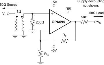 Figure 52. IF Amplifier With Improved Noise Figure
The transformer provides a noiseless voltage gain at the expense of higher source impedance for the OPA695 noninverting input current noise. The input impedance is still set to 50 Ω by the 200-Ω resistor on the transformer secondary. A 1:2 turns ratio transformer will reflect the 200 Ω to the input side as a 50-Ω impedance over the bandwidth of the transformer. Using a 1:2 step-up transformer also reduces the required amplifier gain by 1/2 for any particular desired overall gain.
Table 1, Table 2, and Table 3 summarize the recommended resistor values and resulting noise figures over the desired gain setting for three circuit options for the OPA695 operated as a precision IF amplifier. In each case, RF and RG are adjusted for both best bandwidth and required gain.
In all cases, exact computed values for resistors are shown; in an application, pick standard resistor values that are closest to those in the tables.
Table 1. Noninverting Wideband Operational Amplifier
| GAIN TO LOAD (dB) | RF (Ω) | RG (Ω) | NOISE FIGURE |
|---|---|---|---|
| 6 | 478 | 159 | 17.20 |
| 7 | 468 | 134 | 16.55 |
| 8 | 458 | 113 | 15.95 |
| 9 | 446 | 96 | 15.40 |
| 10 | 433 | 81 | 14.91 |
| 11 | 419 | 68 | 14.47 |
| 12 | 402 | 57 | 14.09 |
| 13 | 384 | 48 | 13.76 |
| 14 | 363 | 40 | 13.23 |
| 15 | 340 | 33 | 13.23 |
| 16 | 314 | 27 | 13.03 |
| 17 | 284 | 21 | 12.86 |
| 18 | 252 | 16 | 12.72 |
| 19 | 215 | 12 | 12.60 |
| 20 | 174 | 9 | 12.51 |
Table 2. Noninverting With a 1:2 Input Step-Up Transformer
| GAIN TO LOAD (dB) | RF (Ω) | RG (Ω) | NOISE FIGURE |
|---|---|---|---|
| 6 | 516 | 518 | 16.34 |
| 7 | 511 | 412 | 15.54 |
| 8 | 506 | 334 | 14.78 |
| 9 | 500 | 275 | 14.07 |
| 10 | 493 | 228 | 13.40 |
| 11 | 486 | 190 | 12.78 |
| 12 | 478 | 160 | 12.21 |
| 13 | 469 | 135 | 11.70 |
| 14 | 458 | 114 | 11.25 |
| 15 | 447 | 96 | 10.85 |
| 16 | 434 | 81 | 10.15 |
| 17 | 419 | 69 | 10.21 |
| 18 | 403 | 58 | 9.96 |
| 19 | 384 | 48 | 9.74 |
| 20 | 364 | 40 | 9.57 |
Table 3. Inverting Wideband RF Amplifier
| GAIN TO LOAD (dB) | Optimum RF (Ω) | RG (Ω) | Input Match RT | NOISE FIGURE |
|---|---|---|---|---|
| 6 | 463.27 | 116 | 87 | 16.94 |
| 7 | 454.61 | 101 | 98 | 16.06 |
| 8 | 444.91 | 88 | 114 | 15.16 |
| 9 | 434.07 | 77 | 142 | 14.23 |
| 10 | 421.95 | 66 | 199 | 13.24 |
| 11 | 408.42 | 57 | 380 | 12.16 |
| 12 | 398.11 | 50 | Infinite | 11.03 |
| 13 | 446.68 | 50 | Infinite | 10.92 |
| 14 | 501.19 | 50 | Infinite | 10.83 |
| 15 | 562.34 | 50 | Infinite | 10.75 |
| 16 | 630.96 | 50 | Infinite | 10.67 |
| 17 | 707.95 | 50 | Infinite | 10.61 |
| 18 | 794.33 | 50 | Infinite | 10.55 |
| 19 | 891.25 | 50 | Infinite | 10.49 |
| 20 | 1000.00 | 50 | Infinite | 10.45 |
8.4 Device Functional Modes
The OPA695 has two functional modes. The first functional mode is accessed by applying a logic 1 (>3.3 V) to the not Disable (Disable bar) pin. In this mode the amplifier is fully enabled and will draw a supply current of 13 mA.
The second functional mode is the disabled state. The disabled state is accessed by applying a logic 0 (<1.8 V) to the not Disable pin. In this mode, the amplifier is fully disabled and draws a current of only 100 µA.