ZHCSI51A May   2018  – June 2018 OPA521

PRODUCTION DATA.  

  1. 特性
  2. 应用
  3. 说明
    1.     Device Images
      1.      OPA521 方框图
  4. 修订历史记录
  5. Pin Configuration and Functions
    1.     Pin Functions
  6. Specifications
    1. 6.1 Absolute Maximum Ratings
    2. 6.2 ESD Ratings
    3. 6.3 Recommended Operating Conditions
    4. 6.4 Thermal Information
    5. 6.5 Electrical Characteristics
    6. 6.6 Electrical Characteristics: Digital
    7. 6.7 Electrical Characteristics: Power Supply
    8. 6.8 Typical Characteristics
  7. Detailed Description
    1. 7.1 Overview
    2. 7.2 Functional Block Diagram
    3. 7.3 Feature Description
      1. 7.3.1 IQSET Pin
      2. 7.3.2 EN Pin
      3. 7.3.3 ILIM Pin Current Limiting
      4. 7.3.4 IFLAG and TFLAG Pins
    4. 7.4 Device Functional Modes
  8. Application and Implementation
    1. 8.1 Application Information
    2. 8.2 Typical Application
      1. 8.2.1 Design Requirements
      2. 8.2.2 Detailed Design Procedure
        1. 8.2.2.1 Interfacing the OPA521 to the AC Mains
          1. 8.2.2.1.1 Low-Voltage Capacitor
          2. 8.2.2.1.2 High-Voltage Capacitor
          3. 8.2.2.1.3 Inductor
          4. 8.2.2.1.4 Line Coupling Transformer
        2. 8.2.2.2 Circuit Protection
      3. 8.2.3 Application Curves
  9. Power Supply Recommendations
  10. 10Layout
    1. 10.1 Layout Guidelines
      1. 10.1.1 Thermal Considerations
    2. 10.2 Layout Example
  11. 11器件和文档支持
    1. 11.1 器件支持
      1. 11.1.1 第三方产品免责声明
    2. 11.2 文档支持
      1. 11.2.1 相关文档
    3. 11.3 接收文档更新通知
    4. 11.4 社区资源
    5. 11.5 商标
    6. 11.6 静电放电警告
    7. 11.7 术语表
  12. 12"机械、封装和可订购信息

封装选项

机械数据 (封装 | 引脚)
散热焊盘机械数据 (封装 | 引脚)
订购信息

Pin Configuration and Functions

RGW Package
20-Pin VQFN With Exposed Thermal Pad
Top View
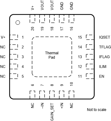
OPA521 SBOSxxx_RGW_OPA521.gif
NC - no internal connection

Pin Functions

PIN I/O DESCRIPTION
NAME NO.
EN 11 I Enables the amplifier (active high, high enables the OPA521)
GAIN_SET 8 I Connect an external resistor to Gain_Set and -IN to increase the gain beyond -7 V/V
GND 16, 17 Ground
IFLAG 13 O Current limit warning flag (open-drain, active high, high signifies current limit condition)
ILIM 12 I Resistor programmable current limit
+IN 9 I Non-inverting input (connect to a voltage equal to (V+)/2)
–IN 7 I Inverting input for closed loop gain = –7 V/V
IQSET 15 I Quiescent current select (active high, high configures the OPA521 to operate in FCC/ARIB bands, low configures the OPA521 to operate in CENELEC Bands A, B, C, D)
NC 2, 3, 4, 5, 6, 10 No internal connection
TFLAG 14 O Thermal limit warning flag (open-drain, active high, high signifies thermal limit condition)
V+ 1, 20 Positive power supply
VOUT 18. 19 O Output
Thermal pad Must be soldered to PCB and connected to GND