ZHCSI51A May 2018 – June 2018 OPA521
PRODUCTION DATA.
8.2.2.1.4 Line Coupling Transformer
Most power-line communication transformers are compact, with turns ratios between 1:1 and 4:1, low leakage inductance, and approximately 1-mH of winding inductance. It is the voltage divider formed by the HV Cap and winding inductance that divides down the ac mains voltage and reduces it to negligible levels at the modem output. Figure 21 shows the equivalent circuit formed with the HV Cap and the line coupling transformer.
 Figure 21. Voltage Divider with HV Cap and Transformer Equivalent Circuit
 Where:
- R1 is the series dc resistance of the primary winding
- R2 is the shunt resistance reflecting losses in the core
- R3 is the series dc resistance of the secondary winding, reflected to the primary side
- L1 is the primary leakage inductance
- L2 is the open circuit inductance of the primary winding
- L3 is the secondary leakage inductance reflected to the primary side
- C1 is the self-capacitance of the primary winding
- C2 is the self-capacitance of the secondary winding reflected to the primary side
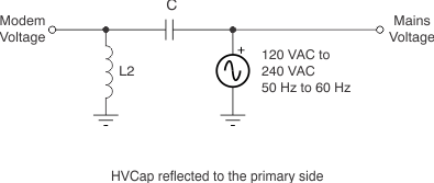
For the purposes of analysis, this circuit can be simplified as shown in Figure 22.
 Figure 22. Simplified AC Mains Voltage Divider
 Where:
- L2 = OCL of the transformer primary
- C = HV Cap reflected to the primary side
In a typical line coupling circuit the ac mains voltage injected into the modem is approximately 20 mVPP.
Determining the optimal turns ratio (N1/N2) for the power-line communication transformer is simple, and based on the principle of using the maximum output swing capability of the power amplifier together with the maximum output current capability of the power amplifier to achieve maximum power transfer efficiency into the load. Assuming the power-supply voltage and target load impedance are known, the turns ratio is determined as shown in Figure 17, and calculated with Equation 11 and Equation 12.