ZHCSH14A November   2017  – December 2017 OPA2333P

PRODUCTION DATA.  

  1. 特性
  2. 应用
  3. 说明
    1.     Device Images
      1.      双向低侧电流分流放大器
      2.      失调电压与温度间的关系
  4. 修订历史记录
  5. Pin Configuration and Functions
    1.     Pin Functions
  6. Specifications
    1. 6.1 Absolute Maximum Ratings
    2. 6.2 ESD Ratings
    3. 6.3 Recommended Operating Conditions
    4. 6.4 Thermal Information: OPA2333P
    5. 6.5 Electrical Characteristics
    6. 6.6 Typical Characteristics
  7. Detailed Description
    1. 7.1 Overview
    2. 7.2 Functional Block Diagram
    3. 7.3 Feature Description
      1. 7.3.1 Operating Voltage
      2. 7.3.2 Input Voltage
      3. 7.3.3 Internal Offset Correction
      4. 7.3.4 Achieving Output Swing to the Op Amp Negative Rail
      5. 7.3.5 Specified Start-Up Performance
      6. 7.3.6 WSON Package
    4. 7.4 Device Functional Modes
  8. Application and Implementation
    1. 8.1 Application Information
    2. 8.2 Typical Application
      1. 8.2.1 Bidirectional Current-Sensing
        1. 8.2.1.1 Design Requirements
        2. 8.2.1.2 Detailed Design Procedure
        3. 8.2.1.3 Application Curve
      2. 8.2.2 High-Side Voltage-to-Current (V-I) Converter
        1. 8.2.2.1 Design Requirements
        2. 8.2.2.2 Detailed Design Procedure
        3. 8.2.2.3 Application Curve
      3. 8.2.3 Other Applications
  9. Power Supply Recommendations
  10. 10Layout
    1. 10.1 Layout Guidelines
      1. 10.1.1 General Layout Guidelines
      2. 10.1.2 WSON (DFN) Layout Guidelines
    2. 10.2 Layout Example
  11. 11器件和文档支持
    1. 11.1 器件支持
      1. 11.1.1 开发支持
    2. 11.2 文档支持
      1. 11.2.1 相关文档
    3. 11.3 接收文档更新通知
    4. 11.4 社区资源
    5. 11.5 商标
    6. 11.6 静电放电警告
    7. 11.7 Glossary
  12. 12机械、封装和可订购信息

封装选项

机械数据 (封装 | 引脚)
散热焊盘机械数据 (封装 | 引脚)
订购信息

Typical Characteristics

Table 1. List of Typical Characteristics

TITLEFIGURE
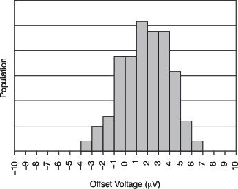
Offset Voltage Production Distribution Figure 1
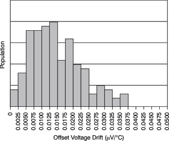
Offset Voltage Drift Production Distribution Figure 2
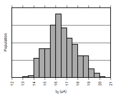
Quiescent Current Production Distribution Figure 3
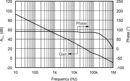
Open-Loop Gain vs Frequency Figure 4
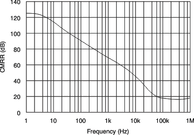
Common-Mode Rejection Ratio vs Frequency Figure 5
Power-Supply Rejection Ratio vs Frequency Figure 6
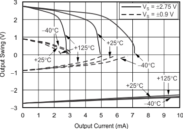
Output Voltage Swing vs Output Current Figure 7
Input Bias Current vs Common-Mode Voltage Figure 8
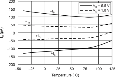
Input Bias Current vs Temperature Figure 9
Quiescent Current vs Temperature Figure 10
Large-Signal Step Response Figure 11
Small-Signal Step Response Figure 12
Positive Overvoltage Recovery Figure 13
Negative Overvoltage Recovery Figure 14
Settling Time vs Closed-Loop Gain Figure 15
Small-Signal Overshoot vs Load Capacitance Figure 16
0.1-Hz to 10-Hz Noise Figure 17
Current and Voltage Noise Spectral Density vs Frequency Figure 18
At TA = 25°C, VS = 5 V, and CL = 0 pF, unless otherwise noted.
OPA2333P tc_histo_bos351.gif
Figure 1. Offset Voltage Production Distribution
OPA2333P tc_histo_drift_bos351.gif
Figure 2. Offset Voltage Drift Production Distribution
OPA2333P Iq_data_hist.gif
VS = 5.5 V
Figure 3. Quiescent Current Production Distribution
OPA2333P tc_cmrr-frq_bos351.gif
Figure 5. Common-Mode Rejection Ratio vs Frequency
OPA2333P tc_vos-io_bos351.gif
Figure 7. Output Voltage Swing vs Output Current
OPA2333P tc_ib-tmp_bos351.gif
Figure 9. Input Bias Current vs Temperature
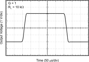
OPA2333P tc_resp_lg_bos351.gif
Figure 11. Large-Signal Step Response
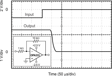
OPA2333P tc_pos_recov_bos351.gif
Figure 13. Positive Overvoltage Recovery
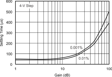
OPA2333P tc_tim-cloop_bos351.gif
Figure 15. Settling Time vs Closed-Loop Gain
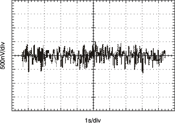
OPA2333P tc_noise_bos351.gif
Figure 17. 0.1-Hz to 10-Hz Noise
OPA2333P tc_oloop-frq_bos351.gif
Figure 4. Open-Loop Gain and Phase vs Frequency
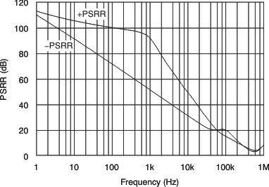
OPA2333P tc_psrr-frq_bos351.gif
Figure 6. Power-Supply Rejection Ratio vs Frequency
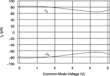
OPA2333P tc_ib-vcm_bos351.gif
Figure 8. Input Bias Current vs Common-Mode Voltage
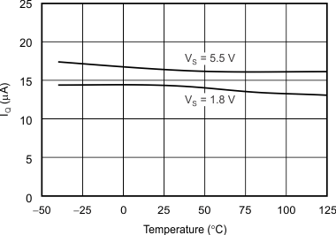
OPA2333P tc_iq-tmp_bos351.gif
Figure 10. Quiescent Current vs Temperature
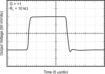
OPA2333P tc_resp_sm_bos351.gif
Figure 12. Small-Signal Step Response
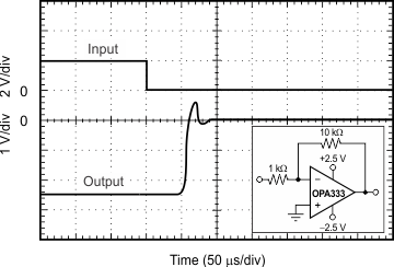
OPA2333P tc_neg_recov_bos351.gif
Figure 14. Negative Overvoltage Recovery
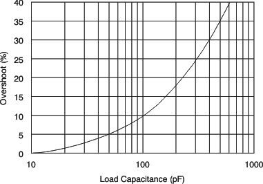
OPA2333P tc_ovrshoot-cl_bos351.gif
Figure 16. Small-Signal Overshoot
vs Load Capacitance
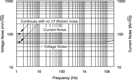
OPA2333P tc_noise-frq_bos351.gif
Figure 18. Current and Voltage Noise Spectral Density vs Frequency