SBOS483I July 2009 – May 2015 OPA2333-HT
PRODUCTION DATA.
- 1 Features
- 2 Applications
- 3 Description
- 4 Revision History
- 5 Pin Configuration and Functions
- 6 Specifications
- 7 Detailed Description
- 8 Application and Implementation
- 9 Power Supply Recommendations
- 10Layout
- 11Device and Documentation Support
- 12Mechanical, Packaging, and Orderable Information
封装选项
机械数据 (封装 | 引脚)
散热焊盘机械数据 (封装 | 引脚)
订购信息
7 Detailed Description
7.1 Overview
The OPA2333 is a Zero-Drift, low-power, rail-to-rail input and output dual operational amplifier. The device operates from 1.8 V to 5.5 V, is unity-gain stable, and is suitable for a wide range of general-purpose applications. The Zero-Drift architecture provides low offset voltage and near zero offset voltage drift.
7.2 Functional Block Diagrams
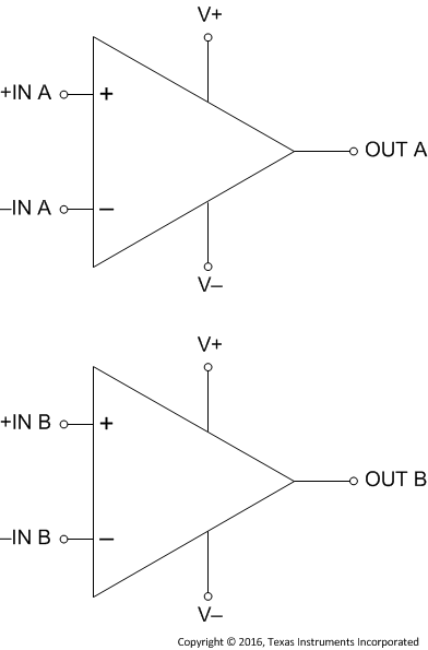
 Figure 19. Functional Block Diagram for A and B Amps
7.3 Feature Description
The OPA2333 is unity-gain stable and free from unexpected output phase reversal. It uses a proprietary auto-calibration technique to provide low offset voltage and very low drift over time and temperature. For lowest offset voltage and precision performance, circuit layout and mechanical conditions should be optimized. Avoid temperature gradients that create thermoelectric (Seebeck) effects in the thermocouple junctions formed from connecting dissimilar conductors. These thermally-generated potentials can be made to cancel by ensuring they are equal on both input terminals. Other layout and design considerations include: (1)
- Use low thermoelectric-coefficient conditions (avoid dissimilar metals)
- Thermally isolate components from power supplies or other heat sources
- Shield operational amplifier and input circuitry from air currents, such as cooling fans
Following these guidelines will reduce the likelihood of junctions being at different temperatures, which can cause thermoelectric voltages of 0.1 μV/°C or higher, depending on materials used.
7.3.1 Operating Voltage
The OPA2333 operational amplifier operates over a power-supply range of 1.8 V to 5.5 V (±0.9 V to
±2.75 V). Supply voltages higher than 7 V (absolute maximum) can permanently damage the device. Parameters that vary over supply voltage or temperature are shown in Typical Characteristics.
7.3.2 Input Voltage
The OPA2333 input common-mode voltage range extends 0.1 V beyond the supply rails. The OPA2333 is designed to cover the full range without the troublesome transition region found in some other rail-to-rail amplifiers.
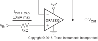
Normally, input bias current is about 70 pA; however, input voltages exceeding the power supplies can cause excessive current to flow into or out of the input pins. Momentary voltages greater than the power supply can be tolerated if the input current is limited to 10 mA. This limitation is easily accomplished with an input resistor (see Figure 20).

7.3.3 Internal Offset Correction
The OPA2333 operational amplifier uses an auto-calibration technique with a time-continuous 350-kHz operational amplifier in the signal path. This amplifier is zero corrected every 8 μs using a proprietary technique. Upon power up, the amplifier requires approximately 100 μs to achieve specified VOS accuracy. This design has no aliasing or flicker noise.
7.3.4 Achieving Output Swing to the Operational Amplifier Negative Rail
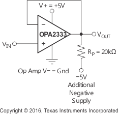
Some applications require output voltage swings from 0 V to a positive full-scale voltage (such as 2.5 V) with excellent accuracy. With most single-supply operational amplifiers, problems arise when the output signal approaches 0 V, near the lower output swing limit of a single-supply operational amplifier. A good single-supply operational amplifier may swing close to single-supply ground, but will not reach ground. The output of the OPA2333 can be made to swing to ground, or slightly below, on a single-supply power source. To do so requires the use of another resistor and an additional, more negative, power supply than the operational amplifier negative supply. A pulldown resistor may be connected between the output and the additional negative supply to pull the output down below the value that the output would otherwise achieve (see Figure 21).
 Figure 21. VOUT Range to Ground
The OPA2333 has an output stage that allows the output voltage to be pulled to its negative supply rail, or slightly below, using the technique previously described. This technique only works with some types of output stages. The OPA2333 has been characterized to perform with this technique; however, the recommended resistor value is approximately 20 kΩ.
NOTE
This configuration will increase the current consumption by several hundreds of microamps.
Accuracy is excellent down to 0 V and as low as –2 mV. Limiting and nonlinearity occurs below –2 mV, but excellent accuracy returns as the output is again driven above –2 mV. Lowering the resistance of the pulldown resistor allows the operational amplifier to swing even further below the negative rail. Resistances as low as 10 kΩ can be used to achieve excellent accuracy down to –10 mV.
7.4 Device Functional Modes
The OPA2333 device has a single functional mode. The device is powered on as long as the power supply voltage is between 1.8 V (±0.9 V) and 5.5 V (±2.75 V).