SBOS483I July 2009 – May 2015 OPA2333-HT
PRODUCTION DATA.
- 1 Features
- 2 Applications
- 3 Description
- 4 Revision History
- 5 Pin Configuration and Functions
- 6 Specifications
- 7 Detailed Description
- 8 Application and Implementation
- 9 Power Supply Recommendations
- 10Layout
- 11Device and Documentation Support
- 12Mechanical, Packaging, and Orderable Information
封装选项
机械数据 (封装 | 引脚)
散热焊盘机械数据 (封装 | 引脚)
订购信息
8 Application and Implementation
NOTE
Information in the following applications sections is not part of the TI component specification, and TI does not warrant its accuracy or completeness. TI’s customers are responsible for determining suitability of components for their purposes. Customers should validate and test their design implementation to confirm system functionality.
8.1 Application Information
The OPA2333 family is a unity-gain stable, precision operational amplifier with very low offset voltage drift; these devices are also free from output phase reversal. Applications with noisy or high-impedance power supplies require decoupling capacitors close to the device power-supply pins. In most cases, 0.1-μF capacitors are adequate.
8.2 Typical Applications
8.2.1 High-Side Voltage-to-Current (V-I) Converter
The circuit shown in Figure 22 is a high-side voltage-to-current (V-I) converter. It translates in input voltage of 0 V to 2 V to and output current of 0 mA to 100 mA. Figure 23 shows the measured transfer function for this circuit. The low offset voltage and offset drift of the OPA2333 facilitate excellent dc accuracy for the circuit.
 Figure 22. High-Side Voltage-to-Current (V-I) Converter
8.2.1.1 Design Requirements
The design requirements are as follows:
- Supply Voltage: 5-V DC
- Input: 0-V to 2-V DC
- Output: 0-mA to 10-mA DC
8.2.1.2 Detailed Design Procedure
The V-I transfer function of the circuit is based on the relationship between the input voltage, VIN, and the three current sensing resistors, RS1, RS2, and RS3. The relationship between VIN and RS1 determines the current that flows through the first stage of the design. The current gain from the first stage to the second stage is based on the relationship between RS2 and RS3.
For a successful design, pay close attention to the DC characteristics of the operational amplifier chosen for the application. To meet the performance goals, this application benefits from an operational amplifier with low offset voltage, low temperature drift, and rail-to-rail output. The OPA2333 CMOS operational amplifier is a high-precision, 5-µV offset, 0.05-μV/°C drift amplifier optimized for low-voltage, single-supply operation with an output swing to within 50 mV of the positive rail. The OPA2333 family uses chopping techniques to provide low initial offset voltage and near-zero drift over time and temperature. Low offset voltage and low drift reduce the offset error in the system, making these devices appropriate for precise DC control. The rail-to-rail output stage of the OPA2333 ensures that the output swing of the operational amplifier is able to fully control the gate of the MOSFET devices within the supply rails.
See TIPD102 for a detailed error analysis, design procedure, and additional measured results.
8.2.1.3 Application Curve
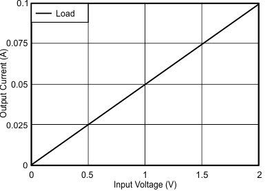 Figure 23. Measured Transfer Function for High-Side V-I Converter
8.2.2 Precision, Low-Level Voltage-to-Current (V-I) Converter
The circuit shown in Figure 24 is a precision, low-level voltage-to-current (V-I) converter. The converter translates in input voltage of 0 V to 5 V and output current of 0 µA to 5 µA. Figure 25 shows the measured transfer function for this circuit. The low offset voltage and offset drift of the OPA2333 facilitate excellent dc accuracy for the circuit. Figure 26 shows the calibrated error for the entire range of the circuit.
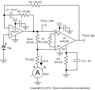 Figure 24. Low-Level, Precision V-I Converter
8.2.2.1 Design Requirements
The design requirements are as follows:
- Supply Voltage: 5-V DC
- Input: 0-V to 5-V DC
- Output: 0-μA to 5-μA DC
8.2.2.2 Detailed Design Procedure
The V-I transfer function of the circuit is based on the relationship between the input voltage, VIN, RSET, and the instrumentation amplifier (INA) gain. During operation, the input voltage divided by the INA gain appears across the set resistor in Equation 1:
The current through RSET must flow through the load, so IOUT is VSET / RSET. IOUT remains a well-regulated current as long as the total voltage across RSET and RLOAD does not violate the output limits of the operational amplifier or the input common-mode limits of the INA. The voltage across the set resistor (VSET) is the input voltage divided by the INA gain (that is, VSET = 1 V / 10 = 0.1 V). The current is determined by VSET and RSET shown in Equation 2:
See TIPD107 for a detailed error analysis, design procedure, and additional measured results.
8.2.2.3 Application Curves
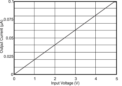 Figure 25. Measured Transfer Function for Low-Level Precision V-I
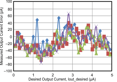 Figure 26. Calibrated Output Error for Low-Level V-I
8.2.3 Composite Amplifier
The circuit shown in Figure 27 is a composite amplifier used to drive the reference on the ADS8881. The OPA2333 provides excellent dc accuracy, and the THS4281 allows the output of the circuit to respond quickly to the transient current requirements of a typical SAR data converter reference input. The ADS8881 system was optimized for THD and achieved a measured performance of –110 dB. The linearity of the ADC is shown Figure 28.
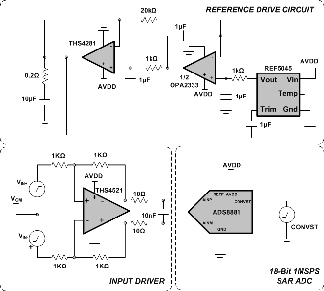 Figure 27. Composite Amplifier Reference Driver Circuit
8.2.3.1 Design Requirements
The design requirements for this block design are:
- System Supply Voltage: 5-V DC
- ADC Supply Voltage: 3.3-V DC
- ADC Sampling Rate: 1 MSPS
- ADC Reference Voltage (VREF): 4.5-V DC
- ADC Input Signal: A differential input signal with amplitude of Vpk = 4.315 V (–0.4 dBFS to avoid clipping) and frequency, fIN = 10 kHz are applied to each differential input of the ADC
8.2.3.2 Detailed Design Procedure
The two primary design considerations to maximize the performance of a high-resolution SAR ADC are the input driver and the reference driver design. The circuit comprises the critical analog circuit blocks, the input driver, anti-aliasing filter, and the reference driver. Each analog circuit block should be carefully designed based on the ADC performance specifications in order to maximize the distortion and noise performance of the data acquisition system while consuming low power. The diagram includes the most important specifications for each individual analog block. This design systematically approaches the design of each analog circuit block to achieve a 16-bit, low-noise and low-distortion data acquisition system for a 10-kHz sinusoidal input signal. The first step in the design requires an understanding of the requirement of extremely low distortion input driver amplifier. This understanding helps in the decision of an appropriate input driver configuration and selection of an input amplifier to meet the system requirements. The next important step is the design of the anti-aliasing RC-filter to attenuate ADC kick-back noise while maintaining the amplifier stability. The final design challenge is to design a high-precision reference driver circuit, which would provide the required value VREF with low offset, drift, and noise contributions.
In designing a very low distortion data acquisition block, it is important to understand the sources of nonlinearity. Both the ADC and the input driver introduce nonlinearity in a data acquisition block. To achieve the lowest distortion, the input driver for a high-performance SAR ADC must have a distortion that is negligible against the ADC distortion. This parameter requires the input driver distortion to be 10 dB lower than the ADC THD. This stringent requirement ensures that overall THD of the system is not degraded by more than –0.5 dB.
It is therefore important to choose an amplifier that meets the above criteria to avoid the system THD from being limited by the input driver. The amplifier nonlinearity in a feedback system depends on the available loop gain. See TIPD115 for a detailed error analysis, design procedure, and additional measured results.
8.2.3.3 Application Curve
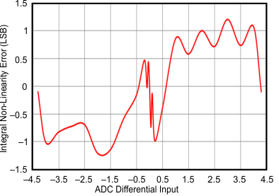 Figure 28. Linearity of the ADC8881 System
8.3 System Examples
8.3.1 Temperature Measurement Application
Figure 29 shows a temperature measurement application.
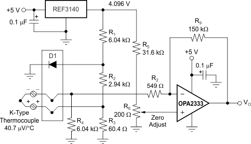 Figure 29. Temperature Measurementf
8.3.2 Single Operational Amplifier Bridge Amplifier Application
Figure 30 shows the basic configuration for a bridge amplifier.
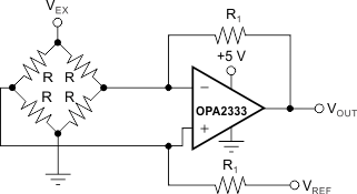 Figure 30. Single Operational Amplifier Bridge Amplifier
8.3.3 Low-Side Current Monitor Application
A low-side current shunt monitor is shown in Figure 31. RN are operational resistors used to isolate the ADS1100 from the noise of the digital I2C bus. The ADS1100 is a 16-bit converter; therefore, a precise reference is essential for maximum accuracy. If absolute accuracy is not required and the 5-V power supply is sufficiently stable, the REF3130 can be omitted.
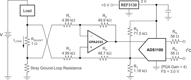
NOTE:
1% resistors provide adequate common-mode rejection at small ground-loop errors.8.3.4 Other Applications
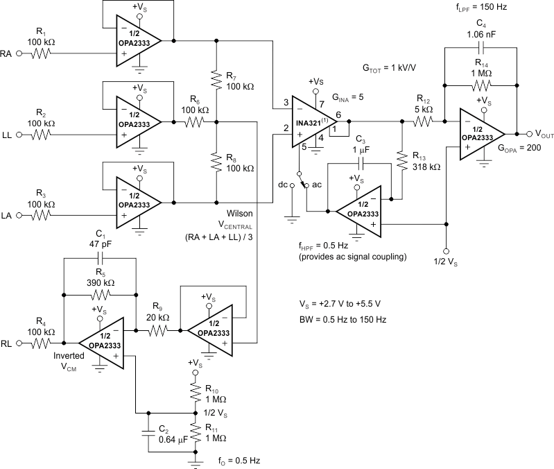
Additional application ideas are shown in Figure 32 through Figure 35.
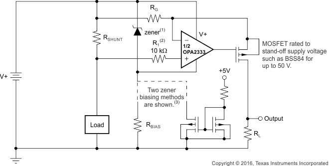
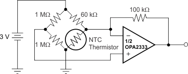 Figure 33. Thermistor Measurement
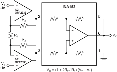 Figure 34. Precision Instrumentation Amplifier
