ZHCS372C August 2011 – June 2016 OPA2188
PRODUCTION DATA.
- 1 特性
- 2 应用范围
- 3 说明
- 4 修订历史记录
- 5 Zero-Drift Amplifier Portfolio
- 6 Pin Configuration and Functions
-
7 Specifications
- 7.1 Absolute Maximum Ratings
- 7.2 ESD Ratings
- 7.3 Recommended Operating Conditions
- 7.4 Thermal Information
- 7.5 Electrical Characteristics: High-Voltage Operation, VS = ±4 V to ±18 V (VS = 8 V to 36 V)
- 7.6 Electrical Characteristics: Low-Voltage Operation, VS = ±2 V to < ±4 V (VS = +4 V to < +8 V)
- 7.7 Typical Characteristics: Table of Graphs
- 7.8 Typical Characteristics
- 8 Detailed Description
- 9 Application and Implementation
- 10Power Supply Recommendations
- 11Layout
- 12器件和文档支持
- 13机械、封装和可订购信息
封装选项
机械数据 (封装 | 引脚)
散热焊盘机械数据 (封装 | 引脚)
- DGK|8
订购信息
9 Application and Implementation
NOTE
Information in the following applications sections is not part of the TI component specification, and TI does not warrant its accuracy or completeness. TI’s customers are responsible for determining suitability of components for their purposes. Customers should validate and test their design implementation to confirm system functionality.
9.1 Application Information
9.2 Typical Applications
9.2.1 High-Side Voltage-to-Current (V-I) Converter
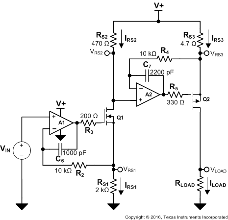
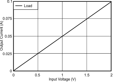
The circuit shown in Figure 44 is a high-side voltage-to-current (V-I) converter. It translates in input voltage of 0 V to 2 V to and output current of 0 mA to 100 mA. Figure 45 shows the measured transfer function for this circuit. The low offset voltage and offset drift of the OPA2188 facilitate excellent dc accuracy for the circuit.
 Figure 44. High-Side Voltage-to-Current (V-I) Converter
9.2.1.1 Design Requirements
The design requirements are as follows:
- Supply Voltage: 5 V DC
- Input: 0 V to 2 V DC
- Output: 0 mA to 100 mA DC
9.2.1.2 Detailed Design Procedure
The V-I transfer function of the circuit is based on the relationship between the input voltage, VIN, and the three current sensing resistors, RS1, RS2, and RS3. The relationship between VIN and RS1 determines the current that flows through the first stage of the design. The current gain from the first stage to the second stage is based on the relationship between RS2 and RS3.
For a successful design, pay close attention to the dc characteristics of the operational amplifier chosen for the application. To meet the performance goals, this application benefits from an operational amplifier with low offset voltage, low temperature drift, and rail-to-rail output. The OPA2188 CMOS operational amplifier is a high-precision, ultra-low offset, ultra-low drift amplifier optimized for low-voltage, single-supply operation with an output swing to within 15 mV of the positive rail. The OPA2188 family uses chopping techniques to provide low initial offset voltage and near-zero drift over time and temperature. Low offset voltage and low drift reduce the offset error in the system, making these devices appropriate for precise dc control. The rail-to-rail output stage of the OPA2188 ensures that the output swing of the operational amplifier is able to fully control the gate of the MOSFET devices within the supply rails.
A detailed error analysis, design procedure, and additional measured results are given in TIPD102.
9.2.1.3 Application Curve
 Figure 45. Measured Transfer Function for High-Side V-I Converter
9.3 System Examples
9.3.1 Discrete INA + Attenuation for ADC With 3.3-V Supply
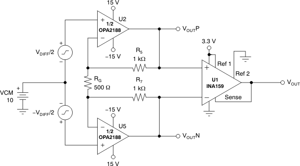
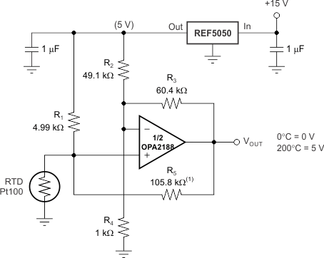
The application examples of Figure 46 and Figure 47 highlight only a few of the circuits where the OPA2188 can be used.
 Figure 46. Discrete INA + Attenuation for ADC with 3.3-V Supply
9.3.2 RTD Amplifier with Linearization

NOINDENT:
R5 provides positive-varying excitation to linearize output.