SLOS070D July 1979 – November 2014 NE5534 , NE5534A , SA5534 , SA5534A
PRODUCTION DATA.
- 1 Features
- 2 Applications
- 3 Description
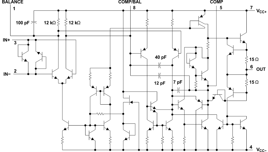
- 4 Simplified Schematic
- 5 Revision History
- 6 Pin Configuration and Functions
- 7 Specifications
- 8 Detailed Description
- 9 Application and Implementation
- 10Power Supply Recommendations
- 11Layout
- 12Device and Documentation Support
- 13Mechanical, Packaging, and Orderable Information
8 Detailed Description
8.1 Overview
The NE5534, NE5534A, SA5534, and SA5534A devices are high-performance operational amplifiers combining excellent dc and ac characteristics. Some of the features include very low noise, high output-drive capability, high unity-gain and maximum-output-swing bandwidths, low distortion, and high slew rate.
These operational amplifiers are compensated internally for a gain equal to or greater than three. Optimization of the frequency response for various applications can be obtained by use of an external compensation capacitor between COMP and COMP/BAL. The devices feature input-protection diodes, output short-circuit protection, and offset-voltage nulling capability with use of the BALANCE and COMP/BAL pins (see the Application Circuit Diagram).
For the NE5534A and SA5534A devices, a maximum limit is specified for the equivalent input noise voltage.
8.2 Functional Block Diagram
8.3 Feature Description
8.3.1 Offset-Voltage Null Capability
The input offset voltage of operational amplifiers (op amps) arises from unavoidable mismatches in the differential input stage of the op-amp circuit caused by mismatched transistor pairs, collector currents, current-gain betas (β), collector or emitter resistors, and so on. The input offset pins allow the designer to adjust for these mismatches by external circuitry. See the Application and Implementation section for more details on design techniques.
8.3.2 Slew Rate
The slew rate is the rate at which an operational amplifier can change its output when there is a change on the input. The NE5534 and SA5534 devices have a 13-V/μs slew rate.
8.3.3 Common-Mode Rejection Ratio
The common-mode rejection ratio (CMRR) of an amplifier is a measure of how well the device rejects unwanted input signals common to both input leads. It is found by taking the ratio of the change in input offset voltage to the change in the input voltage and converting to decibels. Ideally the CMRR is infinite, but in practice, amplifiers are designed to have it as high as possible. The CMRR of the NE5534 and SA5534 devices is 100 dB.
8.3.4 Unity-Gain Bandwidth
The unity-gain bandwidth is the frequency up to which an amplifier with a unity gain may be operated without greatly distorting the signal. The NE5534 and SA5534 devices have a 10-MHz unity-gain bandwidth.
8.3.5 External Compensation Capability
Frequency compensation with a capacitor may be used to increase the gain-bandwidth product (GBW) of the amplifier. See the Application and Implementation section for more details on design techniques.
8.4 Device Functional Modes
The NE5534 and SA5534 devices are powered on when the supply is connected. Each of these devices can be operated as a single supply operational amplifier or dual supply amplifier depending on the application.