ZHCS707D December 2011 – September 2018 MSP430F6720 , MSP430F6721 , MSP430F6723 , MSP430F6724 , MSP430F6725 , MSP430F6726 , MSP430F6730 , MSP430F6731 , MSP430F6733 , MSP430F6734 , MSP430F6735 , MSP430F6736
PRODUCTION DATA.
- 1器件概述
- 2修订历史记录
- 3Device Comparison
- 4Terminal Configuration and Functions
-
5Specifications
- 5.1 Absolute Maximum Ratings
- 5.2 ESD Ratings
- 5.3 Recommended Operating Conditions
- 5.4 Active Mode Supply Current Into VCC Excluding External Current
- 5.5 Low-Power Mode Supply Currents (Into VCC) Excluding External Current
- 5.6 Low-Power Mode With LCD Supply Currents (Into VCC) Excluding External Current
- 5.7 Thermal Resistance Characteristics
- 5.8
Digital I/O Ports
- Table 5-1 Schmitt-Trigger Inputs – General-Purpose I/O
- Table 5-2 Inputs – Ports P1 and P2
- Table 5-3 Leakage Current – General-Purpose I/O
- Table 5-4 Outputs – General-Purpose I/O (Full Drive Strength)
- Table 5-5 Typical Characteristics – General-Purpose I/O (Full Drive Strength)
- Table 5-6 Outputs – General-Purpose I/O (Reduced Drive Strength)
- 5.8.1 Typical Characteristics – General-Purpose I/O (Reduced Drive Strength)
- Table 5-7 Output Frequency – General-Purpose I/O
- 5.9 Clock Specifications
- 5.10 Power-Management Module (PMM)
- 5.11
Auxiliary Supplies
- Table 5-19 Auxiliary Supplies, Recommended Operating Conditions
- Table 5-20 Auxiliary Supplies, AUXVCC3 (Backup Subsystem) Currents
- Table 5-21 Auxiliary Supplies, Auxiliary Supply Monitor
- Table 5-22 Auxiliary Supplies, Switch ON-Resistance
- Table 5-23 Auxiliary Supplies, Switching Time
- Table 5-24 Auxiliary Supplies, Switch Leakage
- Table 5-25 Auxiliary Supplies, Auxiliary Supplies to ADC10_A
- Table 5-26 Auxiliary Supplies, Charge Limiting Resistor
- 5.12 Timer_A
- 5.13 eUSCI
- 5.14 LCD Controller
- 5.15
SD24_B
- Table 5-36 SD24_B Power Supply and Recommended Operating Conditions
- Table 5-37 SD24_B Analog Input
- Table 5-38 SD24_B Supply Currents
- Table 5-39 SD24_B Performance
- Table 5-40 SD24_B AC Performance
- Table 5-41 SD24_B AC Performance
- Table 5-42 SD24_B AC Performance
- Table 5-43 SD24_B External Reference Input
- 5.16 ADC10_A
- 5.17 REF
- 5.18 Flash Memory
- 5.19 Emulation and Debug
-
6Detailed Description
- 6.1 CPU
- 6.2 Instruction Set
- 6.3 Operating Modes
- 6.4 Interrupt Vector Addresses
- 6.5 Memory Organization
- 6.6 Bootloader (BSL)
- 6.7 JTAG Operation
- 6.8 Flash Memory
- 6.9 RAM
- 6.10 Backup RAM
- 6.11
Peripherals
- 6.11.1 Oscillator and System Clock
- 6.11.2 Power Management Module (PMM)
- 6.11.3 Auxiliary Supply System
- 6.11.4 Backup Subsystem
- 6.11.5 Digital I/O
- 6.11.6 Port Mapping Controller
- 6.11.7 System Module (SYS)
- 6.11.8 Watchdog Timer (WDT_A)
- 6.11.9 DMA Controller
- 6.11.10 CRC16
- 6.11.11 Hardware Multiplier
- 6.11.12 Enhanced Universal Serial Communication Interface (eUSCI)
- 6.11.13 ADC10_A
- 6.11.14 SD24_B
- 6.11.15 TA0
- 6.11.16 TA1
- 6.11.17 TA2
- 6.11.18 TA3
- 6.11.19 SD24_B Triggers
- 6.11.20 ADC10_A Triggers
- 6.11.21 Real-Time Clock (RTC_C)
- 6.11.22 Reference (REF) Module Voltage Reference
- 6.11.23 LCD_C
- 6.11.24 Embedded Emulation Module (EEM) (S Version)
- 6.11.25 Peripheral File Map
- 6.12
Input/Output Diagrams
- 6.12.1 Port P1 (P1.0 and P1.1) Input/Output With Schmitt Trigger (MSP430F67xxIPZ and MSP430F67xxIPN)
- 6.12.2 Port P1 (P1.2) Input/Output With Schmitt Trigger (MSP430F67xxIPZ and MSP430F67xxIPN)
- 6.12.3 Port P1 (P1.3 to P1.5) Input/Output With Schmitt Trigger (MSP430F67xxIPZ and MSP430F67xxIPN)
- 6.12.4 Port P1 (P1.6 and P1.7) (MSP430F67xxIPZ and MSP430F67xxIPN), Port P2 (P2.0 and P2.1) (MSP430F67xxIPZ Only) Input/Output With Schmitt Trigger
- 6.12.5 Port P2 (P2.2 to P2.7) Input/Output With Schmitt Trigger (MSP430F67xxIPZ Only)
- 6.12.6 Port P3 (P3.0 to P3.3) Input/Output With Schmitt Trigger (MSP430F67xxIPZ Only)
- 6.12.7 Port P3 (P3.4 to P3.7) Input/Output With Schmitt Trigger (MSP430F67xxIPZ Only)
- 6.12.8 Port P4 (P4.0 to P4.7), Port P5 (P5.0 to P5.7), Port P6 (P6.0 to P6.7), Port P7 (P7.0 to P7.7), Port P8 (P8.0 to P8.3) Input/Output With Schmitt Trigger (MSP430F67xxIPZ Only)
- 6.12.9 Port P8 (P8.4 to P8.7) Input/Output With Schmitt Trigger (MSP430F67xxIPZ Only)
- 6.12.10 Port P9 (P9.0) Input/Output With Schmitt Trigger (MSP430F67xxIPZ Only)
- 6.12.11 Port P9 (P9.1 to P9.3) Input/Output With Schmitt Trigger (MSP430F67xxIPZ Only)
- 6.12.12 Port P2 (P2.0 and P2.1) Input/Output With Schmitt Trigger (MSP430F67xxIPN Only)
- 6.12.13 Port P2 (P2.2 to P2.7) Input/Output With Schmitt Trigger (MSP430F67xxIPN Only)
- 6.12.14 Port P3 (P3.0 to P3.7) Input/Output With Schmitt Trigger (MSP430F67xxIPN Only)
- 6.12.15 Port P4 (P4.0 to P4.7), Port P5 (P5.0 to P5.7), Port P6 (P6.0 to P6.7) Input/Output With Schmitt Trigger (MSP430F67xxIPN Only)
- 6.12.16 Port PJ (PJ.0) JTAG Pin TDO, Input/Output With Schmitt Trigger or Output
- 6.12.17 Port PJ (PJ.1 to PJ.3) JTAG Pins TMS, TCK, TDI/TCLK, Input/Output With Schmitt Trigger or Output
- 6.13 Device Descriptors (TLV)
- 7器件和文档支持
- 8机械、封装和可订购信息
Table 5-21 Auxiliary Supplies, Auxiliary Supply Monitor
over operating free-air temperature range (unless otherwise noted)| PARAMETER | TEST CONDITIONS | VCC | MIN | TYP | MAX | UNIT | |
|---|---|---|---|---|---|---|---|
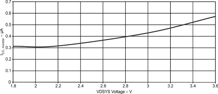
| ICC,Monitor | Average supply current for monitoring circuitry drawn from VDSYS | LOCKAUX = 0, AUXMRx = 0,
AUX0MD = 0, AUX1MD = 0, AUX2MD = 1, VDSYS = DVCC, VASYS = AVCC, Current measured at VDSYS pin (also see Figure 5-11) |
3 V | 0.70 | µA | ||
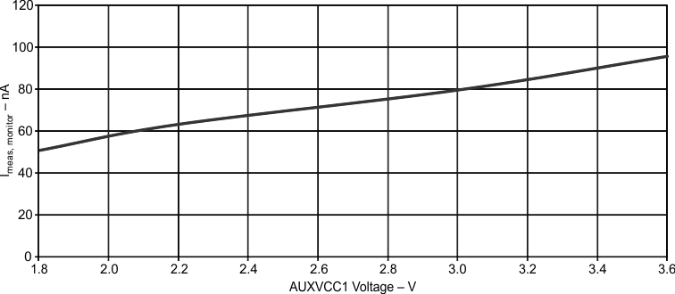
| IMeas,Monitor | Average current drawn from monitored supply during measurement cycle | LOCKAUX = 0, AUXMRx = 0,
AUX0MD = 0, AUX1MD = 0, AUX2MD = 1, VDSYS = DVCC, VASYS = AVCC, AUXVCC1 = 3 V, Current measured at AUXVCC1 pin (also see Figure 5-12) |
0.11 | µA | |||
| VMonitor | Auxiliary supply threshold level | AUXLVLx = 0 | 1.67 | 1.74 | 1.80 | V | |
| AUXLVLx = 1 | 1.87 | 1.95 | 2.01 | ||||
| AUXLVLx = 2 | 2.06 | 2.14 | 2.21 | ||||
| AUXLVLx = 3 | 2.19 | 2.27 | 2.33 | ||||
| AUXLVLx = 4 | 2.33 | 2.41 | 2.48 | ||||
| AUXLVLx = 5 | 2.63 | 2.72 | 2.79 | ||||
| AUXLVLx = 6 | 2.91 | 3.02 | 3.10 | ||||
| AUXLVLx = 7 | 2.91 | 3.02 | 3.10 | ||||
 Figure 5-11 VDSYS Voltage vs ICC,Monitor
  Figure 5-12 AUXVCC1 Voltage vs IMeas,Monitor
 Table 5-22 lists the ON-resistance characteristics of the auxiliary supplies.