ZHCSGU2A July 2017 – September 2017 LP5569
PRODUCTION DATA.
- 1 特性
- 2 应用
- 3 说明
- 4 修订历史记录
- 5 Device Comparison Table
- 6 Pin Configuration and Functions
-
7 Specifications
- 7.1 Absolute Maximum Ratings
- 7.2 ESD Ratings
- 7.3 Recommended Operating Conditions
- 7.4 Thermal Information
- 7.5 Electrical Characteristics
- 7.6 Charge-Pump Electrical Characteristics
- 7.7 LED Current Sinks Electrical Characteristics
- 7.8 Logic Interface Characteristics
- 7.9 Timing Requirements (EN/PWM)
- 7.10 Serial-Bus Timing Requirements (SDA, SCL), See
- 7.11 External Clock Timing Requirements (CLK), See
- 7.12 Typical Characteristics
-
8 Detailed Description
- 8.1 Overview
- 8.2 Functional Block Diagram
- 8.3 Feature Description
- 8.4 Device Functional Modes
- 8.5 Programming
- 8.6
Register Maps
- 8.6.1
LP5569_MAP Registers
- 8.6.1.1 CONFIG Register (Address = 0h) [reset = 0h]
- 8.6.1.2 LED_ENGINE_CONTROL1 Register (Address = 1h) [reset = 0h]
- 8.6.1.3 LED_ENGINE_CONTROL2 Register (Address = 2h) [reset = 0h]
- 8.6.1.4 LED0_CONTROL Register (Address = 7h) [reset = 0h]
- 8.6.1.5 LED1_CONTROL Register (Address = 8h) [reset = 0h]
- 8.6.1.6 LED2_CONTROL Register (Address = 9h) [reset = 0h]
- 8.6.1.7 LED3_CONTROL Register (Address = Ah) [reset = 0h]
- 8.6.1.8 LED4_CONTROL Register (Address = Bh) [reset = 0h]
- 8.6.1.9 LED5_CONTROL Register (Address = Ch) [reset = 0h]
- 8.6.1.10 LED6_CONTROL Register (Address = Dh) [reset = 0h]
- 8.6.1.11 LED7_CONTROL Register (Address = Eh) [reset = 0h]
- 8.6.1.12 LED8_CONTROL Register (Address = Fh) [reset = 0h]
- 8.6.1.13 LED0_PWM Register (Address = 16h) [reset = 0h]
- 8.6.1.14 LED1_PWM Register (Address = 17h) [reset = 0h]
- 8.6.1.15 LED2_PWM Register (Address = 18h) [reset = 0h]
- 8.6.1.16 LED3_PWM Register (Address = 19h) [reset = 0h]
- 8.6.1.17 LED4_PWM Register (Address = 1Ah) [reset = 0h]
- 8.6.1.18 LED5_PWM Register (Address = 1Bh) [reset = 0h]
- 8.6.1.19 LED6_PWM Register (Address = 1Ch) [reset = 0h]
- 8.6.1.20 LED7_PWM Register (Address = 1Dh) [reset = 0h]
- 8.6.1.21 LED8_PWM Register (Address = 1Eh) [reset = 0h]
- 8.6.1.22 LED0_CURRENT Register (Address = 22h) [reset = AFh]
- 8.6.1.23 LED1_CURRENT Register (Address = 23h) [reset = AFh]
- 8.6.1.24 LED2_CURRENT Register (Address = 24h) [reset = AFh]
- 8.6.1.25 LED3_CURRENT Register (Address = 25h) [reset = AFh]
- 8.6.1.26 LED4_CURRENT Register (Address = 26h) [reset = AFh]
- 8.6.1.27 LED5_CURRENT Register (Address = 27h) [reset = AFh]
- 8.6.1.28 LED6_CURRENT Register (Address = 28h) [reset = AFh]
- 8.6.1.29 LED7_CURRENT Register (Address = 29h) [reset = AFh]
- 8.6.1.30 LED8_CURRENT Register (Address = 2Ah) [reset = AFh]
- 8.6.1.31 MISC Register (Address = 2Fh) [reset = 40h]
- 8.6.1.32 ENGINE1_PC Register (Address = 30h) [reset = 0h]
- 8.6.1.33 ENGINE2_PC Register (Address = 31h) [reset = 0h]
- 8.6.1.34 ENGINE3_PC Register (Address = 32h) [reset = 0h]
- 8.6.1.35 MISC2 Register (Address = 33h) [reset = 2h]
- 8.6.1.36 ENGINE_STATUS Register (Address = 3Ch) [reset = 80h]
- 8.6.1.37 IO_CONTROL Register (Address = 3Dh) [reset = 2h]
- 8.6.1.38 VARIABLE_D Register (Address = 3Eh) [reset = 0h]
- 8.6.1.39 RESET Register (Address = 3Fh) [reset = 0h]
- 8.6.1.40 ENGINE1_VARIABLE_A Register (Address = 42h) [reset = 0h]
- 8.6.1.41 ENGINE2_VARIABLE_A Register (Address = 43h) [reset = 0h]
- 8.6.1.42 ENGINE3_VARIABLE_A Register (Address = 44h) [reset = 0h]
- 8.6.1.43 MASTER_FADER1 Register (Address = 46h) [reset = 0h]
- 8.6.1.44 MASTER_FADER2 Register (Address = 47h) [reset = 0h]
- 8.6.1.45 MASTER_FADER3 Register (Address = 48h) [reset = 0h]
- 8.6.1.46 MASTER_FADER_PWM Register (Address = 4Ah) [reset = 0h]
- 8.6.1.47 ENGINE1_PROG_START Register (Address = 4Bh) [reset = 0h]
- 8.6.1.48 ENGINE2_PROG_START Register (Address = 4Ch) [reset = 0h]
- 8.6.1.49 ENGINE3_PROG_START Register (Address = 4Dh) [reset = 0h]
- 8.6.1.50 PROG_MEM_PAGE_SELECT Register (Address = 4Fh) [reset = 0h]
- 8.6.1.51 PROGRAM_MEM_00 Register (Address = 50h) [reset = 0h]
- 8.6.1.52 PROGRAM_MEM_01 Register (Address = 51h) [reset = 0h]
- 8.6.1.53 PROGRAM_MEM_02 Register (Address = 52h) [reset = 0h]
- 8.6.1.54 PROGRAM_MEM_03 Register (Address = 53h) [reset = 0h]
- 8.6.1.55 PROGRAM_MEM_04 Register (Address = 54h) [reset = 0h]
- 8.6.1.56 PROGRAM_MEM_05 Register (Address = 55h) [reset = 0h]
- 8.6.1.57 PROGRAM_MEM_06 Register (Address = 56h) [reset = 0h]
- 8.6.1.58 PROGRAM_MEM_07 Register (Address = 57h) [reset = 0h]
- 8.6.1.59 PROGRAM_MEM_08 Register (Address = 58h) [reset = 0h]
- 8.6.1.60 PROGRAM_MEM_09 Register (Address = 59h) [reset = 0h]
- 8.6.1.61 PROGRAM_MEM_10 Register (Address = 5Ah) [reset = 0h]
- 8.6.1.62 PROGRAM_MEM_11 Register (Address = 5Bh) [reset = 0h]
- 8.6.1.63 PROGRAM_MEM_12 Register (Address = 5Ch) [reset = 0h]
- 8.6.1.64 PROGRAM_MEM_13 Register (Address = 5Dh) [reset = 0h]
- 8.6.1.65 PROGRAM_MEM_14 Register (Address = 5Eh) [reset = 0h]
- 8.6.1.66 PROGRAM_MEM_15 Register (Address = 5Fh) [reset = 0h]
- 8.6.1.67 PROGRAM_MEM_16 Register (Address = 60h) [reset = 0h]
- 8.6.1.68 PROGRAM_MEM_17 Register (Address = 61h) [reset = 0h]
- 8.6.1.69 PROGRAM_MEM_18 Register (Address = 62h) [reset = 0h]
- 8.6.1.70 PROGRAM_MEM_19 Register (Address = 63h) [reset = 0h]
- 8.6.1.71 PROGRAM_MEM_20 Register (Address = 64h) [reset = 0h]
- 8.6.1.72 PROGRAM_MEM_21 Register (Address = 65h) [reset = 0h]
- 8.6.1.73 PROGRAM_MEM_22 Register (Address = 66h) [reset = 0h]
- 8.6.1.74 PROGRAM_MEM_23 Register (Address = 67h) [reset = 0h]
- 8.6.1.75 PROGRAM_MEM_24 Register (Address = 68h) [reset = 0h]
- 8.6.1.76 PROGRAM_MEM_25 Register (Address = 69h) [reset = 0h]
- 8.6.1.77 PROGRAM_MEM_26 Register (Address = 6Ah) [reset = 0h]
- 8.6.1.78 PROGRAM_MEM_27 Register (Address = 6Bh) [reset = 0h]
- 8.6.1.79 PROGRAM_MEM_28 Register (Address = 6Ch) [reset = 0h]
- 8.6.1.80 PROGRAM_MEM_29 Register (Address = 6Dh) [reset = 0h]
- 8.6.1.81 PROGRAM_MEM_30 Register (Address = 6Eh) [reset = 0h]
- 8.6.1.82 PROGRAM_MEM_31 Register (Address = 6Fh) [reset = 0h]
- 8.6.1.83 ENGINE1_MAPPING1 Register (Address = 70h) [reset = 0h]
- 8.6.1.84 ENGINE1_MAPPING2 Register (Address = 71h) [reset = 0h]
- 8.6.1.85 ENGINE2_MAPPING1 Register (Address = 72h) [reset = 0h]
- 8.6.1.86 ENGINE2_MAPPING2 Register (Address = 73h) [reset = 0h]
- 8.6.1.87 ENGINE3_MAPPING1 Register (Address = 74h) [reset = 0h]
- 8.6.1.88 ENGINE3_MAPPING2 Register (Address = 75h) [reset = 0h]
- 8.6.1.89 PWM_CONFIG Register (Address = 80h) [reset = 4h]
- 8.6.1.90 LED_FAULT1 Register (Address = 81h) [reset = 0h]
- 8.6.1.91 LED_FAULT2 Register (Address = 82h) [reset = 0h]
- 8.6.1.92 GENERAL_FAULT Register (Address = 83h) [reset = 4h]
- 8.6.1
LP5569_MAP Registers
- 9 Application and Implementation
- 10Power Supply Recommendations
- 11Layout
- 12器件和文档支持
- 13机械、封装和可订购信息
7 Specifications
7.1 Absolute Maximum Ratings
over operating ambient temperature range (unless otherwise noted)(1)| MIN | MAX | UNIT | ||
|---|---|---|---|---|
| Voltage on VIN, CLK, ADDR, EN/PWM, GPIO/TRIG/INT, SCL, SDA, VOUT(2) | –0.3 | 6 | V | |
| Voltage on LED0 to LED8, C1–, C2–, C1+, C2+ | −0.3 | VVIN + 0.3 V with 6 V max. | V | |
| Voltage on V1P8 | −0.3 | 2 | V | |
| Continuous power dissipation | Internally limited | Internally limited | ||
| Junction temperature, TJ-MAX | –40 | 125 | °C | |
| Storage temperature, Tstg | −65 | 150 | °C | |
(1) Stresses beyond those listed under Absolute Maximum Ratings may cause permanent damage to the device. These are stress ratings only, which do not imply functional operation of the device at these or any other conditions beyond those indicated under Recommended Operating Conditions. Exposure to absolute-maximum-rated conditions for extended periods may affect device reliability.
(2) VOUT cannot be forced to a power supply during device shutdown.
7.2 ESD Ratings
| VALUE | UNIT | |||
|---|---|---|---|---|
| V(ESD) | Electrostatic discharge | Human-body model (HBM), per ANSI/ESDA/JEDEC JS-001(1) | ±2500 | V |
| Charged-device model (CDM), per JEDEC specification JESD22-C101(2) | ±250 | |||
(1) JEDEC document JEP155 states that 500-V HBM allows safe manufacturing with a standard ESD control process.
(2) JEDEC document JEP157 states that 250-V CDM allows safe manufacturing with a standard ESD control process.
7.3 Recommended Operating Conditions
over operating ambient temperature range (unless otherwise noted)| MIN | MAX | UNIT | ||
|---|---|---|---|---|
| Input voltage on VIN | 2.5 | 5.5 | V | |
| Voltage on LED0 to LED8, C1–, C2–, C1+, C2+, VOUT | 0 | VVIN | V | |
| Voltage on CLK, ADDR, EN/PWM, GPIO/TRIG/INT, SDA, SCL | 0 | VVIN | V | |
| Input voltage on V1P8 | 1.65 | 1.95 | V | |
| Output current on VOUT | 0 | 160 | mA | |
| Operating ambient temperature, TA (1) | −40 | 85 | °C | |
(1) In applications where high power dissipation and/or poor PCB cooling status is present, the maximum ambient temperature might require derating. Maximum ambient temperature (TA-MAX) is dependent on the maximum operating junction temperature (TJ-MAX-OP = 125°C), the maximum power dissipation of the device in the application (PD-MAX), and the junction-to ambient thermal resistance of the device in the application (RθJA), as given by the equation: TA-MAX = TJ-MAX-OP – (RθJA × PD-MAX).
7.4 Thermal Information
| THERMAL METRIC(1) | LP5569 | UNIT | |
|---|---|---|---|
| RTW (WQFN) | |||
| 24 PINS | |||
| RθJA | Junction-to-ambient thermal resistance | 35.8 | °C/W |
| RθJC(top) | Junction-to-case (top) thermal resistance | 26.7 | °C/W |
| RθJB | Junction-to-board thermal resistance | 13.1 | °C/W |
| ψJT | Junction-to-top characterization parameter | 0.4 | °C/W |
| ψJB | Junction-to-board characterization parameter | 13.1 | °C/W |
| RθJC(bot) | Junction-to-case (bottom) thermal resistance | 4.6 | °C/W |
(1) For more information about traditional and new thermal metrics, see Semiconductor and IC Package Thermal Metrics.
7.5 Electrical Characteristics
Unless otherwise noted, specifications apply to the LP5569 device in a circuit per the typical application diagram for the single device with VVIN = 3.6 V, V1P8 = 1.8 V, VEN/PWM = VVIN, CIN = COUT = CFLY1 = CFLY2 = 1 µF. Typical (TYP) values apply for TA = 25°C and minimum (MIN) and maximum (MAX) apply over the operating ambient temperature range (−40°C < TA < 85°C).| PARAMETER | TEST CONDITIONS | MIN | TYP | MAX | UNIT | |
|---|---|---|---|---|---|---|
| IVIN | Standby supply current | VEN/PWM = 0 V, chip_en (bit) = 0 | 0.2 | 1 | µA | |
| VEN/PWM = 3.3 V, chip_en (bit) = 0, external CLK not running | 1 | 2 | ||||
| VEN/PWM = 3.3 V, chip_en (bit) = 0, external CLK running | 2 | 4 | ||||
| Normal-mode supply current | External CLK running, charge pump and current sinks disabled | 56 | 70 | µA | ||
| Charge pump in 1× mode, no load, current sinks disabled | 65 | 90 | ||||
| Charge pump in 1.5× mode, no load, current-sink outputs disabled | 1.8 | mA | ||||
| Power-save mode supply current | External CLK running, see Automatic Power-Save Mode | 10 | 15 | µA | ||
| Internal oscillator running | 10 | 15 | ||||
| IV1P8 | Standby supply current | VEN/PWM = 0 V, chip_en(bit) = 0 | 0.2 | 1 | µA | |
| VEN/PWM = 3.3 V, chip_en (bit) = 0, external CLK not running | 0.2 | 2 | µA | |||
| VEN/PWM = 3.3 V, chip_en (bit) = 0, external CLK running | 1 | 4 | µA | |||
| Normal-mode supply current | External CLK running, charge pump and current sinks disabled | 174 | 190 | µA | ||
| Charge pump in 1× mode, no load, current sinks disabled | 174 | 190 | µA | |||
| Charge pump in 1.5× mode, no load, current-sink- outputs disabled | 180 | µA | ||||
| Powersave-mode supply current | External CLK running | 1 | 5 | µA | ||
| Internal oscillator running | 1 | 5 | µA | |||
| ƒOSC | 32-kHz internal oscillator frequency accuracy | TA = 25°C | –10% | 10% | ||
| 10-MHz internal oscillator frequency accuracy | –7% | 7% | ||||
| VUVLO | Undervoltage lockout | VVIN falling | 2.2 | V | ||
| VVIN rising | 2.3 | |||||
7.6 Charge-Pump Electrical Characteristics
| PARAMETER | TEST CONDITIONS | MIN | TYP | MAX | UNIT | |
|---|---|---|---|---|---|---|
| ROUT | Charge-pump output resistance | Gain = 1×, VVIN = 4.2 V | 1 | Ω | ||
| Gain = 1.5×, VVIN = 3.7 V | 3.5 | |||||
| VOUT | VVIN = 3.7 V, IOUT = 160 mA, gain = 1.5× | 4.41 | 4.5 | 4.59 | V | |
| ƒSW | Switching frequency | 1.25 | MHz | |||
| ICL | Output current limit | VOUT = 0 V, VVIN = 3.7 V, CP_CONFIG = 0xFF | 600 | mA | ||
| tON | VOUT turnon time | IOUT = 0 mA, VIN ≥ 3 V, VOUT > 4.1 V, gain = 1.5× | 100 | µs | ||
| IOUT | Maximum output current | VVIN > 3.1 V, VOUT dropped 10%, gain = 1.5× | 200 | mA | ||
| VIN > 2.5 V, VOUT dropped 10%, gain = 1.5× | 150 | |||||
7.7 LED Current Sinks Electrical Characteristics
| PARAMETER | TEST CONDITIONS | MIN | TYP | MAX | UNIT | |
|---|---|---|---|---|---|---|
| ILEAKAGE | Leakage current (LED0 to LED8) | PWM = 0%, VLED = 5 V | 1 | µA | ||
| IMAX | Maximum sink current | 24.5 | 25.5 | 26.5 | mA | |
| ILED_ACC | Sink current accuracy(1) | Current set to 17.5 mA. PWM = 100% | –4.5% | 4.5% | ||
| ILED_MATCH | Matching(1) | Current set to 17.5 mA | 1% | 2.5% | ||
| ƒLED | LED switching frequency | 19.5 | kHz | |||
| VSAT | Saturation voltage(2) | Output current set to 25.5 mA | 90 | 110 | mV | |
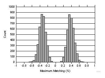
(1) Output-current accuracy is the difference between the actual value of the output current and the programmed value of this current. Matching is the maximum difference from the average. For the constant-current outputs on the device (LED0 to LED8), the following are determined: the maximum output current (MAX), the minimum output current (MIN), and the average output current of all outputs (AVG). The matching number is calculated: (MAX – MIN) / AVG. The typical specification provided is the most likely norm of the matching figure for all devices. Note that some manufacturers have different definitions in use.
(2) Saturation voltage is defined as the voltage when the LED current has dropped 10% from the value measured at 1 V.
7.8 Logic Interface Characteristics
| PARAMETER | TEST CONDITIONS | MIN | TYP | MAX | UNIT | |
|---|---|---|---|---|---|---|
| LOGIC INPUT (EN/PWM, SCL, ADDR) | ||||||
| VIL | Input low level | 0.4 | V | |||
| VIH | Input high level | 1.25 | V | |||
| Ilkg | Input leakage current | VI ≤ VVIN | –1 | 1 | µA | |
| LOGIC OUTPUT (SDA, GPIO/TRIG/INT, CLK) | ||||||
| VIL | Input low level | Pin configured as input | 0.4 | V | ||
| VIH | Input high level | Pin configured as input | 1.25 | V | ||
| Ilkg | Input leakage current | Pin configured as input, VVIN = 5.5 V, VI ≤ VVIN | –1 | 1 | µA | |
| VOL | Output low level | IPULLUP = 3 mA | 0.2 | 0.5 | V | |
| IL | Output leakage current | Pin configured as output, Hi-Z state | 1 | µA | ||
7.9 Timing Requirements (EN/PWM)
| MIN | TYP | MAX | UNIT | ||
|---|---|---|---|---|---|
| tEN | Enable time, EN/PWM first rising edge until first I2C access | 2 | 3 | ms | |
| tEN_TIMEOUT | EN timeout, EN/PWM = low time while in standby mode (enable function) | 15 | ms | ||
| tPWM_TIMEOUT | PWM timeout, EN/PWM = low time while in normal mode (PWM function) | 15 | ms | ||
| PWMres | Resolution for EN/PWM input when configured as PWM, fPWM =10 kHz | 10 | bits | ||
7.10 Serial-Bus Timing Requirements (SDA, SCL), See Figure 1
I2C fast mode| MIN | MAX | UNIT | ||
|---|---|---|---|---|
| ƒSCL | Clock frequency | 0 | 400 | kHz |
| 1 | Hold time (repeated) START condition | 0.6 | µs | |
| 2 | Clock low time | 1.3 | µs | |
| 3 | Clock high time | 600 | ns | |
| 4 | Setup time for a repeated START condition | 600 | ns | |
| 5 | Data hold time | 0 | ns | |
| 6 | Data setup time | 100 | ns | |
| 7 | Rise time of SDA and SCL | 20 + 0.1Cb | 300 | ns |
| 8 | Fall time of SDA and SCL | 15 + 0.1Cb | 300 | ns |
| 9 | Setup time for STOP condition | 600 | ns | |
| 10 | Bus-free time between a STOP and a START condition | 1.3 | µs | |
| Cb | Capacitive load for each bus line | 10 | 200 | pF |
7.11 External Clock Timing Requirements (CLK), See Figure 2
over operating ambient temperature range (unless otherwise noted)| MIN | TYP | MAX | UNIT | |||
|---|---|---|---|---|---|---|
| ƒCLK | Clock frequency | 32.7 | kHz | |||
| tCLKH | High time | 6 | µs | |||
| tCLKL | Low time | 6 | µs | |||
| tr | Clock rise time, 10% rising edge to 90% rising edge | 2 | µs | |||
| tf | Clock fall time, 90% falling edge to 10% falling edge | 2 | µs | |||
 Figure 1. Timing Parameters
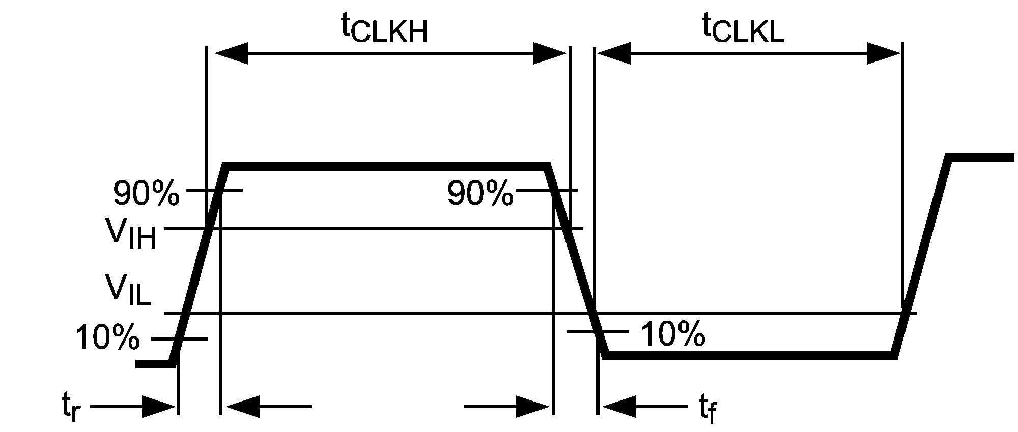 Figure 2. External Clock Signal
7.12 Typical Characteristics
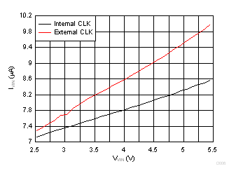
Unless otherwise specified: VVIN = 3.6 V, CIN = COUT = 1 μF, C1 = C2 = 1 μF, TA = 25°C. CIN, COUT, C1, C2: Low-ESR surface-mount ceramic capacitors (MLCCs) used in setting electrical characteristics.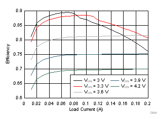
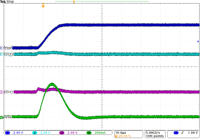
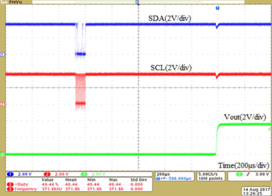
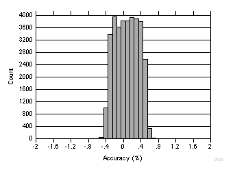
| ILEDx setting per channel = 17.5 mA | ||
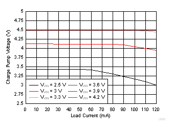
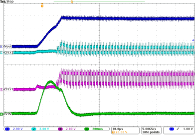
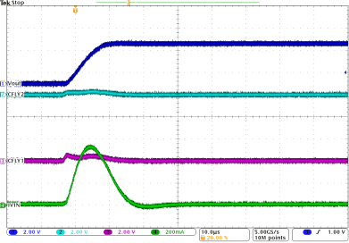
| ILEDx setting per channel = 17.5 mA | ||