SNVS522I August 2007 – August 2015 LP38501-ADJ , LP38503-ADJ
PRODUCTION DATA.
- 1 Features
- 2 Applications
- 3 Description
- 4 Revision History
- 5 Pin Configurations and Functions
- 6 Specifications
- 7 Detailed Description
- 8 Application and Implementation
- 9 Power Supply Recommendations
- 10Layout
- 11Device and Documentation Support
- 12Mechanical, Packaging, and Orderable Information
封装选项
机械数据 (封装 | 引脚)
散热焊盘机械数据 (封装 | 引脚)
- KTT|5
订购信息
1 Features
- Input Voltage: 2.7 V to 5.5 V
- Adjustable Output Voltage: 0.6 V to 5 V
- FlexCap: Stable with Ceramic, Tantalum, or Aluminum Capacitors
- Stable With 10-µF Input and Output Capacitors
- Low Ground-Pin Current
- 25-nA Quiescent Current in Shutdown Mode
- Ensured Output Current of 3 A
- Ensured VADJ Accuracy of ±1.5% at 25°C (A Grade)
- Ensured Accuracy of ±3.5% at 25°C (STD)
- Overtemperature and Overcurrent Protection
- ENABLE (EN) Pin (LP38501 only)
- –40°C to +125°C Operating Temperature Range
2 Applications
- ASIC Power Supplies In:
- Printers, Graphics Cards, DVD Players
- Set Top Boxes, Copiers, Routers
- DSP and FPGA Power Supplies
- SMPS Regulator
- Conversion from 3.3-V or 5-V Rail
3 Description
TI's FlexCap low-dropout (LDO) linear regulators feature unique compensation that allow use of any type of output capacitor with no limits on minimum or maximum equivalent series resistance (ESR). The LP38501 and LP38503 series of LDOs operate from a 2.7-V to 5.5-V input supply. These ultra-low-dropout linear regulators respond very quickly to step changes in load, making them suitable for low-voltage microprocessor applications. Developed on a CMOS process (utilizing a PMOS pass transistor) the LP38501-ADJ and LP38503-ADJ have low quiescent currents that change little with load current.
- GND Pin Current: Typically 2 mA at 3-A load current.
- Disable Mode: Typically 25-nA quiescent current when the EN pin is pulled low.
- Simplified Compensation: Stable with any type of output capacitor, regardless of ESR.
- Precision Output: A grade versions available with 1.5% VADJ tolerance (25°C) and 3% over line, load, and temperature.
Device Information(1)
| PART NUMBER | PACKAGE | BODY SIZE (NOM) |
|---|---|---|
| LP38501 LP38503 |
DDPAK/TO-263 (5) | 10.16 mm x 8.42 mm |
| TO-263 (5) | 10.16 mm x 9.85 mm |
- For all available packages, see the orderable addendum at the end of the data sheet.

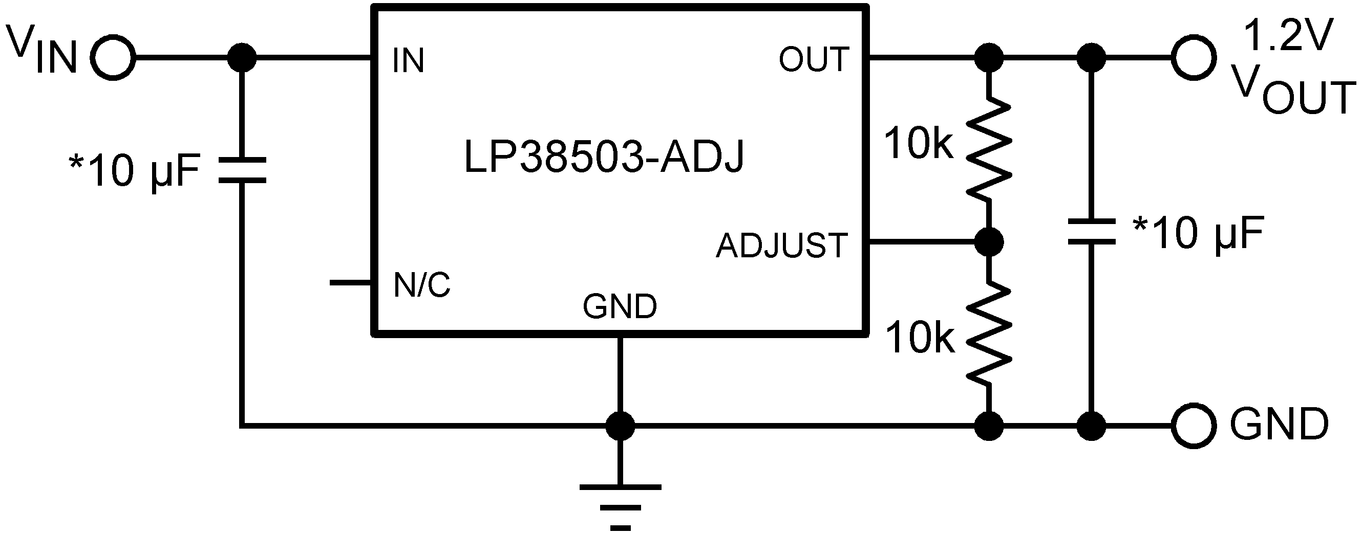
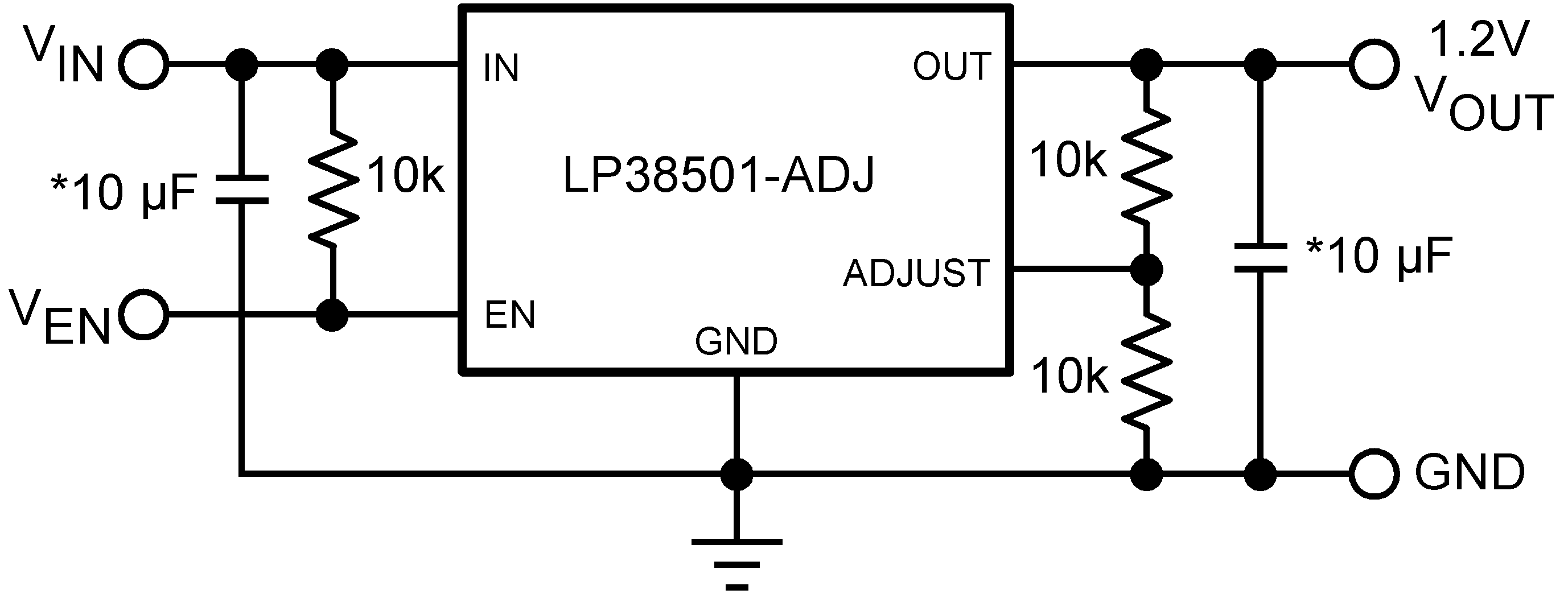
*Minimum capacitance required (see Application and Implementation).
