ZHCSEU9C March   2016  – June 2018 LMZ34202

PRODUCTION DATA.  

  1. 特性
  2. 应用
  3. 说明
    1.     Device Images
      1.      简化应用
      2.      效率与输出电流间的关系
  4. 修订历史记录
  5. Pin Configuration and Functions
    1.     Pin Functions
  6. Specifications
    1. 6.1 Absolute Maximum Ratings
    2. 6.2 ESD Ratings
    3. 6.3 Recommended Operating Conditions
    4. 6.4 Thermal Information
    5. 6.5 Electrical Characteristics
    6. 6.6 Switching Characteristics
    7. 6.7 Typical Characteristics
    8. 6.8 Typical Characteristics (Thermal Derating)
  7. Detailed Description
    1. 7.1 Overview
    2. 7.2 Functional Block Diagram
    3. 7.3 Feature Description
      1. 7.3.1  Adjusting the Output Voltage
      2. 7.3.2  Switching Frequency (RT)
      3. 7.3.3  Recommended Operating Range
      4. 7.3.4  Synchronization (CLK)
      5. 7.3.5  Output Capacitor Selection
      6. 7.3.6  VERSA-COMP Pin Configurations
      7. 7.3.7  Input Capacitor Selection
      8. 7.3.8  Output On/Off Inhibit (INH/UVLO)
      9. 7.3.9  Under Voltage Lockout (UVLO)
      10. 7.3.10 Remote Sense
      11. 7.3.11 VBSEL
      12. 7.3.12 Soft-Start (SS/TR)
      13. 7.3.13 Power Good (PWRGD) and Pull-up (PWRGD_PU)
      14. 7.3.14 Overcurrent Protection
      15. 7.3.15 Thermal Shutdown
    4. 7.4 Device Functional Modes
      1. 7.4.1 Active Mode
      2. 7.4.2 Light Load Operation
      3. 7.4.3 Shutdown Mode
  8. Application and Implementation
    1. 8.1 Application Information
    2. 8.2 Typical Application
      1. 8.2.1 Minimum External Component Application
        1. 8.2.1.1 Design Requirements
        2. 8.2.1.2 Detailed Design Procedure
          1. 8.2.1.2.1 Custom Design With WEBENCH® Tools
          2. 8.2.1.2.2 Output Voltage Set-Point
          3. 8.2.1.2.3 RT and RTSEL
          4. 8.2.1.2.4 VERSA-COMP
          5. 8.2.1.2.5 VBSEL
          6. 8.2.1.2.6 Input Capacitors
          7. 8.2.1.2.7 Output Capacitors
        3. 8.2.1.3 Application Curves
      2. 8.2.2 INH Control Application
        1. 8.2.2.1 Design Requirements
      3. 8.2.3 Detailed Design Procedure
        1. 8.2.3.1 Switching Frequency
        2. 8.2.3.2 Power Good
        3. 8.2.3.3 Inhibit Control
        4. 8.2.3.4 VERSA-COMP
        5. 8.2.3.5 VBSEL
        6. 8.2.3.6 Soft-Start Capacitors
        7. 8.2.3.7 Input Capacitors
        8. 8.2.3.8 Output Capacitors
  9. Power Supply Recommendations
  10. 10Layout
    1. 10.1 Layout Guidelines
    2. 10.2 Layout Example
    3. 10.3 EMI
  11. 11器件和文档支持
    1. 11.1 器件支持
      1. 11.1.1 开发支持
        1. 11.1.1.1 使用 WEBENCH® 工具创建定制设计
      2. 11.1.2 第三方产品免责声明
    2. 11.2 接收文档更新通知
    3. 11.3 社区资源
    4. 11.4 商标
    5. 11.5 静电放电警告
    6. 11.6 术语表
  12. 12机械、封装和可订购信息

封装选项

机械数据 (封装 | 引脚)
散热焊盘机械数据 (封装 | 引脚)
订购信息

VERSA-COMP Pin Configurations

The versa-comp feature of the LMZ34202 allows a simple method to adjust the internal compensation network to provide the optimized phase and gain margin based on the output voltage. This easy-to-use feature requires no external components and is implemented by the simple configuration of two adjacent pins on the module.

The versa-comp feature must be configured in one of two ways; VERSA-COMP pin left OPEN or VERSA-COMP pin tied to VADJ. The output voltage determines the appropriate Versa-Comp pin configuration. Table 8 lists the Versa-Comp configuration. Figure 19 shows the two possible Versa-Comp pin configurations.
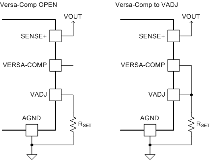
LMZ34202 LMZ36002_VC_3Config.gifFigure 19. Versa-Comp Configurations

Table 8. VERSA-COMP Pin Configurations

VOUT RANGE (V) VERSA-COMP PIN CONFIGURATION
MIN MAX
2.5 < 3.0 OPEN
3.0 7.5 Connect to VADJ