ZHCSI24O September   2000  – April 2018 LMV7235 , LMV7239

PRODUCTION DATA.  

  1. 特性
  2. 应用
  3. 说明
    1.     Device Images
      1.      电源电流与电源电压间的关系
      2.      传播延迟与过驱动
  4. 修订历史记录
  5. Pin Configuration and Functions
    1.     Pin Functions
  6. Specifications
    1. 6.1 Absolute Maximum Ratings
    2. 6.2 ESD Ratings
    3. 6.3 Recommended Operating Conditions
    4. 6.4 Thermal Information
    5. 6.5 Electrical Characteristics, 2.7 V
    6. 6.6 Electrical Characteristics, 5 V
    7. 6.7 Typical Characteristics
  7. Detailed Description
    1. 7.1 Overview
    2. 7.2 Functional Block Diagram
    3. 7.3 Feature Description
      1. 7.3.1 Input Stage
      2. 7.3.2 Output Stage: LMV7239
      3. 7.3.3 Output Stage: LMV7235
    4. 7.4 Device Functional Modes
      1. 7.4.1 Capacitive and Resistive Loads
      2. 7.4.2 Noise
      3. 7.4.3 Hysteresis
        1. 7.4.3.1 Inverting Comparator With Hysteresis
        2. 7.4.3.2 Non-Inverting Comparator With Hysteresis
      4. 7.4.4 Zero Crossing Detector
        1. 7.4.4.1 Zero Crossing Detector With Hysteresis
      5. 7.4.5 Threshold Detector
  8. Application and Implementation
    1. 8.1 Application Information
    2. 8.2 Typical Applications
      1. 8.2.1 Square Wave Oscillator
        1. 8.2.1.1 Design Requirements
        2. 8.2.1.2 Detailed Design Procedure
        3. 8.2.1.3 Application Curves
      2. 8.2.2 Crystal Oscillator
      3. 8.2.3 Infrared (IR) Receiver
      4. 8.2.4 Window Detector
  9. Power Supply Recommendations
  10. 10Layout
    1. 10.1 Layout Guidelines
    2. 10.2 Layout Example
  11. 11器件和文档支持
    1. 11.1 器件支持
      1. 11.1.1 开发支持
    2. 11.2 文档支持
      1. 11.2.1 相关文档
    3. 11.3 相关链接
    4. 11.4 接收文档更新通知
    5. 11.5 社区资源
    6. 11.6 商标
    7. 11.7 静电放电警告
    8. 11.8 术语表
  12. 12机械、封装和可订购信息

封装选项

机械数据 (封装 | 引脚)
散热焊盘机械数据 (封装 | 引脚)
订购信息

Detailed Design Procedure

The maximum frequency is limited by the large signal propagation delay of the comparator and by the capacitive loading at the output, which limits the output slew rate.
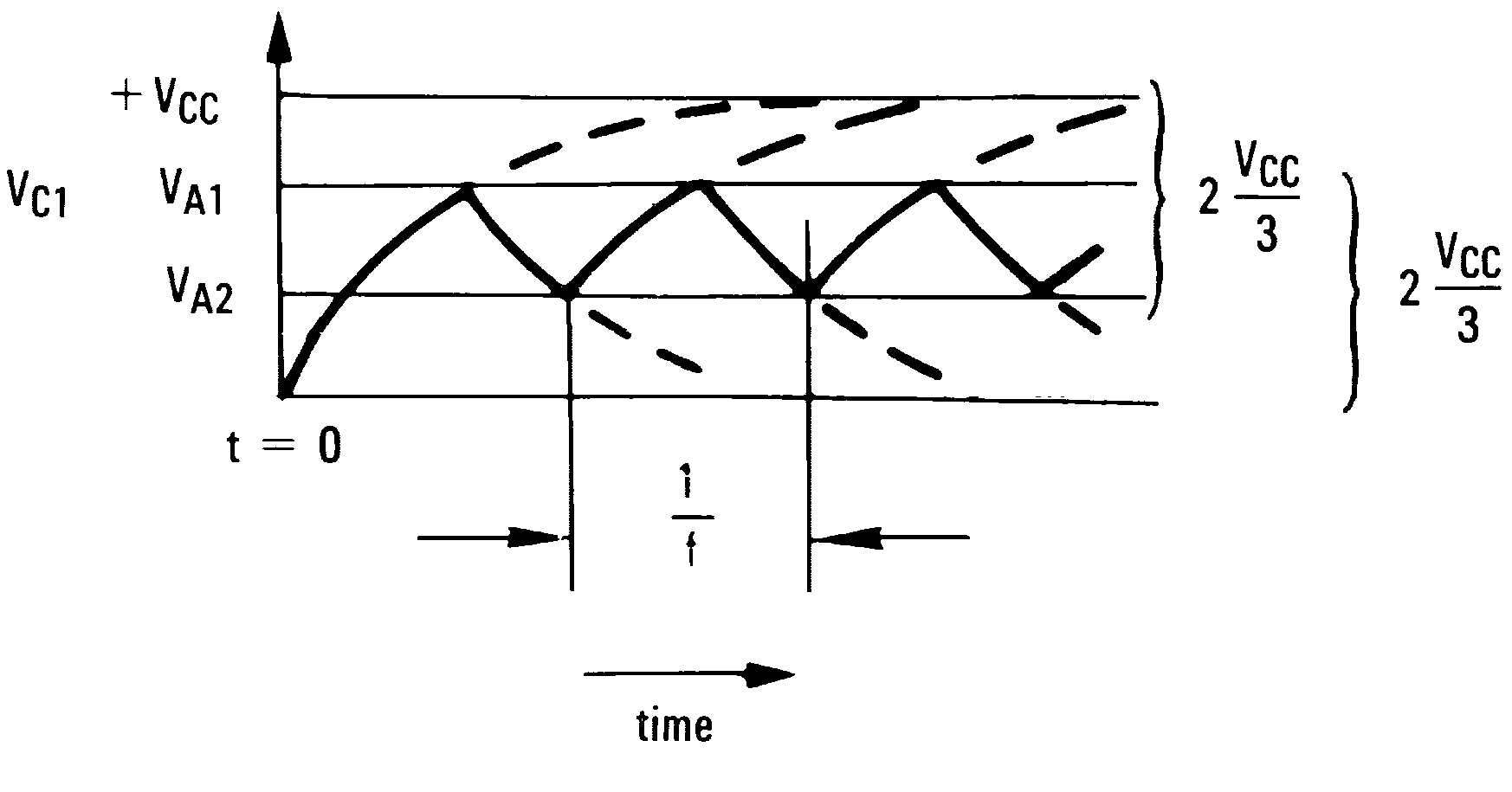
LMV7235 LMV7239 20201339.pngFigure 26. Square Wave Oscillator Timing Thresholds

Consider the output of Figure 25 to be high to analyze the circuit. That implies that the inverted input (VC) is lower than the noninverting input (VA). This causes the C1 to be charged through R4, and the voltage VC increases until it is equal to the noninverting input. The value of VA at this point is:

Equation 8. LMV7235 LMV7239 eq05_snoscz2.gif

If R1 = R2 = R3, then V A1 = 2 Vcc/3

At this point the comparator switches pulling down the output to the negative rail. The value of VA at this point is:

Equation 9. LMV7235 LMV7239 eq06_snoscz2.gif

If R1 = R2 = R3, then VA2 = VCC/3.

The capacitor C1 now discharges through R4, and the voltage VC decreases until it is equal to VA2, at which point the comparator switches again, bringing it back to the initial stage. The time period is equal to twice the time it takes to discharge C1 from 2VCC/3 to VCC/3, which is given by R4C1·ln2. Hence the formula for the frequency is:

Equation 10. F = 1/(2·R4·C1·ln2)

The LMV7239 should be used for a symmetrical output. The LMV7235 will require a pullup resistor on the output to function, and will have a slightly asymmetrical output due to the reduced sourcing current.