SNOS458I April 2000 – June 2016 LMV7219
PRODUCTION DATA.
6 Specifications
6.1 Absolute Maximum Ratings
over operating free-air temperature range (unless otherwise noted) (1)(10)| MIN | MAX | UNIT | ||||
|---|---|---|---|---|---|---|
| Differential input voltage | ± Supply Voltage | |||||
| Output short circuit duration | See(2) | |||||
| Supply voltage (V+ - V−) | 5.5 | V | ||||
| Soldering information | Infrared or Convection (20 sec) | 260 | °C | |||
| Wave Soldering (10 sec) | 260 (lead temp) | °C | ||||
| Voltage at input/output pins | (V+) + 0.4 (V−) − 0.4 |
V | ||||
| Current at input pin(8) | ±10 | mA | ||||
| Maximum junction temperature | 150 | °C | ||||
| Storage temperature | −65 | 150 | °C | |||
6.2 ESD Ratings
| VALUE | UNIT | |||
|---|---|---|---|---|
| V(ESD) | Electrostatic discharge | Human-body model (HBM), per ANSI/ESDA/JEDEC JS-001(1) | ±2000 | V |
| Charged-device model (CDM), per JEDEC specification JESD22-C101(2) | ±150 | |||
(1) JEDEC document JEP155 states that 500-V HBM allows safe manufacturing with a standard ESD control process. Manufacturing with less than 500-V HBM is possible with the necessary precautions. Pins listed as ±2000 V may actually have higher performance.
(2) JEDEC document JEP157 states that 250-V CDM allows safe manufacturing with a standard ESD control process. Manufacturing with less than 250-V CDM is possible with the necessary precautions. Pins listed as ±150 V may actually have higher performance.
6.3 Recommended Operating Conditions
over operating free-air temperature range (unless otherwise noted)| MIN | MAX | UNIT | ||
|---|---|---|---|---|
| Supply voltages (V+ - V−) | 2.7 | 5 | V | |
| Ambient Temperature(3) | −40 | +85 | °C | |
| Junction Temperature | 125 | °C | ||
| PCB Temperature | 105 | °C | ||
6.4 Thermal Information
| THERMAL METRIC(1) | LMV7219 | LMV7219 | UNIT | |
|---|---|---|---|---|
| DBV (SOT23) | DCK (SC70) | |||
| 5 PINS | 5 PINS | |||
| RθJA | Junction-to-ambient thermal resistance | 209 | 296 | °C/W |
| RθJC(top) | Junction-to-case (top) thermal resistance | 170 | 132 | °C/W |
| RθJB | Junction-to-board thermal resistance | 68 | 76 | °C/W |
| ψJT | Junction-to-top characterization parameter | 52 | 8.6 | °C/W |
| ψJB | Junction-to-board characterization parameter | 68 | 75 | °C/W |
| RθJC(bot) | Junction-to-case (bottom) thermal resistance | N/A | N/A | °C/W |
(1) For more information about traditional and new thermal metrics, see the Semiconductor and IC Package Thermal Metrics application report, SPRA953.
6.5 Electrical Characteristics 2.7 V
Unless otherwise specified, all limits ensured for TJ = 25°C, VCM = V+/2, V+ = 2.7 V, V− = 0 V, CL = 10 pF and RL > 1MΩ to V−.| PARAMETER | TEST CONDITIONS | MIN | TYP(4) | MAX(5) | UNIT | ||
|---|---|---|---|---|---|---|---|
| VOS | Input offset voltage | 1 | 6 | mV | |||
| −40°C ≤ TJ ≤ +85°C and TPCB ≤ 105°C | 8 | ||||||
| IB | Input bias current | 450 | 950 | nA | |||
| −40°C ≤ TJ ≤ +85°C and TPCB ≤ 105°C | 2000 | ||||||
| IOS | Input offset current | 50 | 200 | nA | |||
| −40°C ≤ TJ ≤ +85°C and TPCB ≤ 105°C | 400 | ||||||
| CMRR | Common mode rejection ratio | 0 V < VCM < 1.50 V | 62 | 85 | dB | ||
| −40°C ≤ TJ ≤ +85°C and TPCB ≤ 105°C | 55 | ||||||
| PSRR | Power supply rejection ratio | V+ = 2.7 V to 5 V | 65 | 85 | dB | ||
| −40°C ≤ TJ ≤ +85°C and TPCB ≤ 105°C | 55 | ||||||
| VCM | Input common-voltage range | CMRR > 50 dB | VCC −1.2 | VCC −1 | V | ||
| −40°C ≤ TJ ≤ +85°C and TPCB ≤ 105°C | VCC −1.3 | ||||||
| −0.2 | −0.1 | ||||||
| −40°C ≤ TJ ≤ +85°C and TPCB ≤ 105°C | 0 | ||||||
| VO | Output swing high | IL = 4 mA, VID = 500 mV |
VCC −0.3 | VCC −0.22 | V | ||
| −40°C ≤ TJ ≤ +85°C and TPCB ≤ 105°C | VCC −0.4 | ||||||
| IL = 0.4 mA, VID = 500 mV |
VCC −0.05 | VCC −0.02 | |||||
| −40°C ≤ TJ ≤ +85°C and TPCB ≤ 105°C | VCC −0.15 | ||||||
| Output swing low | IL = −4 mA, VID = −500 mV |
130 | 200 | mV | |||
| −40°C ≤ TJ ≤ +85°C and TPCB ≤ 105°C | 300 | ||||||
| IL = −0.4 mA, VID = −500 mV |
15 | 50 | |||||
| −40°C ≤ TJ ≤ +85°C and TPCB ≤ 105°C | 150 | ||||||
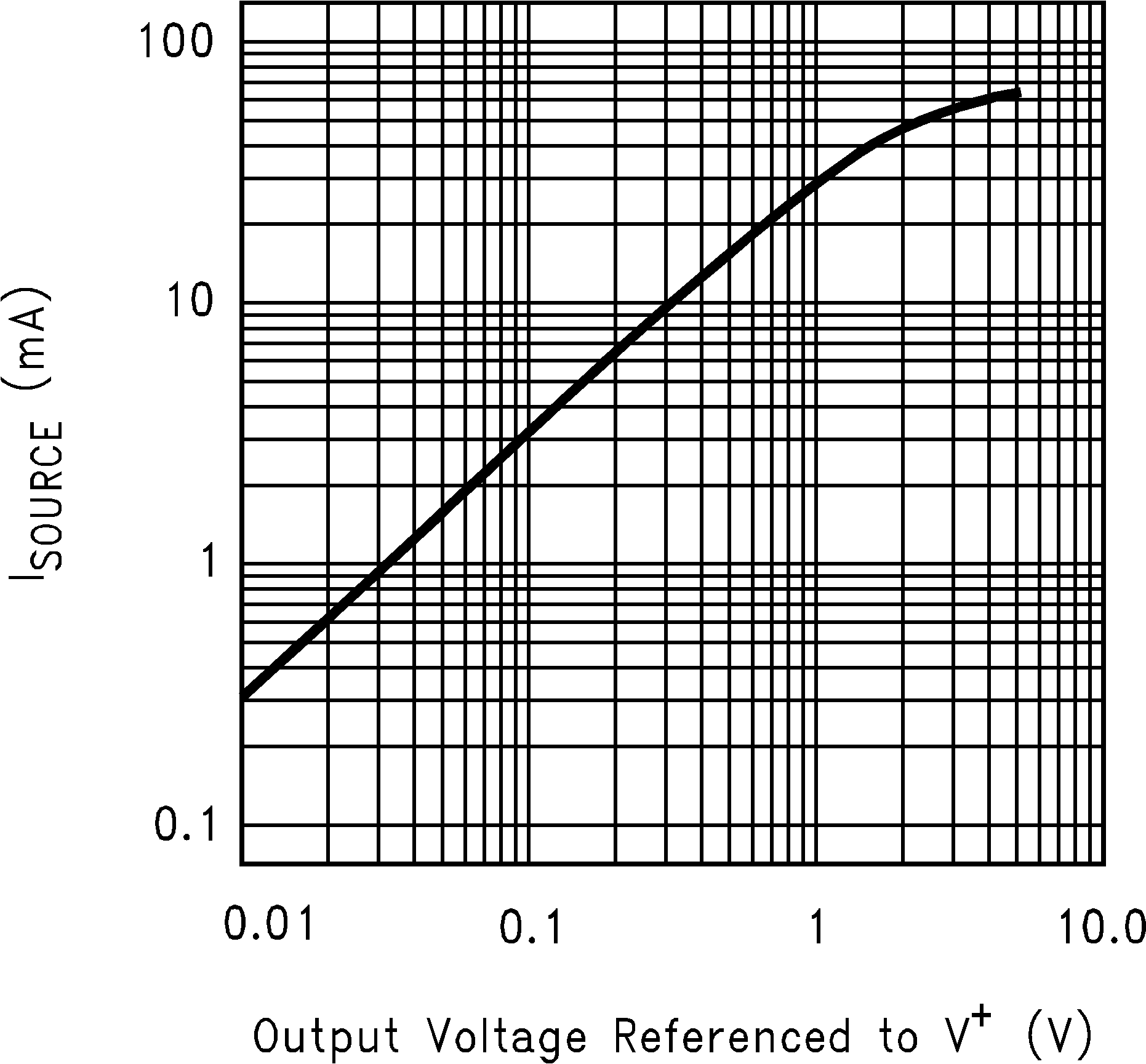
| ISC | Output short circuit current | Sourcing, VO = 0 V(2) | 20 | mA | |||
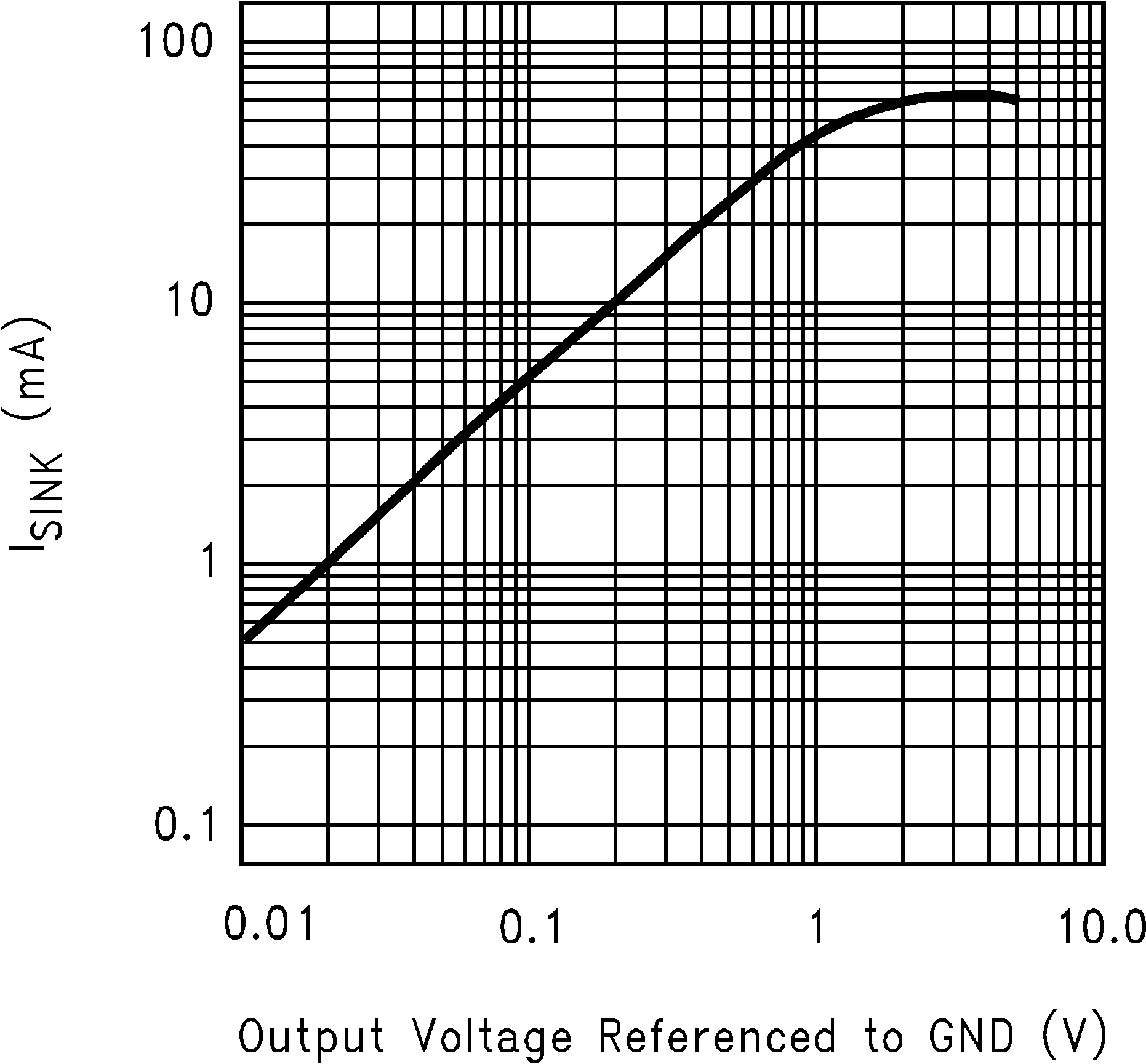
| Sinking, VO = 2.7 V(2) | 20 | ||||||
| IS | Supply current | No Load | 0.9 | 1.6 | mA | ||
| −40°C ≤ TJ ≤ +85°C and TPCB ≤ 105°C | 2.2 | ||||||
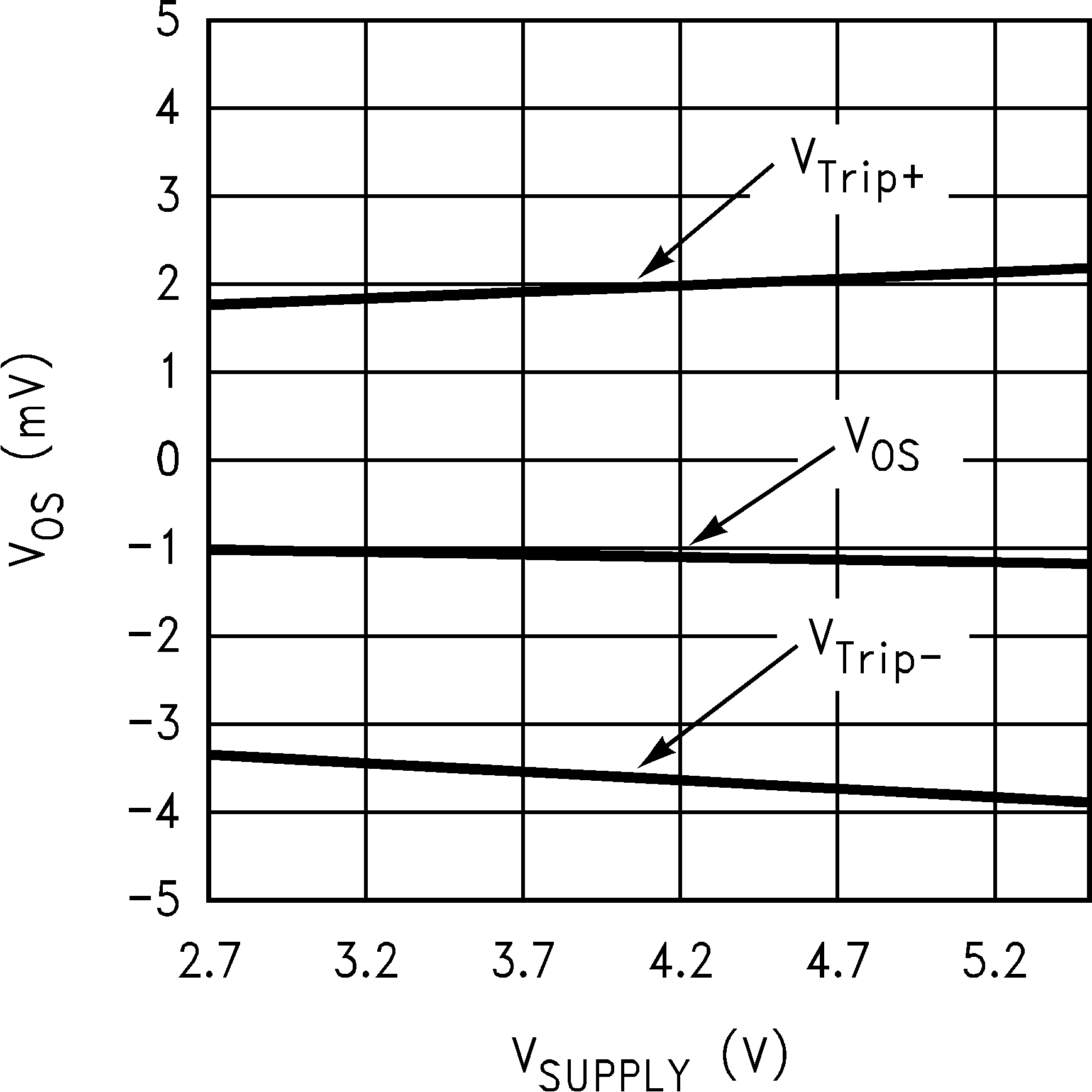
| VHYST | Input hysteresis voltage | See(9) | 7 | mV | |||
| VTRIP+ | Input referred positive trip point | (see Figure 19) | 3 | 8 | mV | ||
| VTRIP− | Input referred negative trip point | (see Figure 19) | −8 | −4 | mV | ||
| tPD | Propagation delay | Overdrive = 5 mV, VCM = 0V(6) | 12 | ns | |||
| Overdrive = 15 mV, VCM = 0 V(6) | 11 | ||||||
| Overdrive = 50 mV, VCM = 0 V(6) | 10 | 20 | |||||
| tSKEW | Propagation delay skew | See(7) | 1 | ns | |||
| tr | Output rise time | 10% to 90% | 2.5 | ns | |||
| tf | Output fall time | 90% to 10% | 2 | ns | |||
6.6 Electrical Characteristics 5 V
Unless otherwise specified, all limits ensured for TJ = 25°C, VCM = V+/2, V+ = 5 V, V− = 0 V, CL = 10 pF and RL > 1 MΩ to V−.| PARAMETER | TEST CONDITIONS | MIN | TYP(4) | MAX(5) | UNIT | ||
|---|---|---|---|---|---|---|---|
| VOS | Input offset voltage | 1 | 6 | mV | |||
| −40°C ≤ TJ ≤ +85°C and TPCB ≤ 105°C | 8 | ||||||
| IB | Input bias current | 500 | 950 | nA | |||
| −40°C ≤ TJ ≤ +85°C and TPCB ≤ 105°C | 2000 | ||||||
| IOS | Input offset current | 50 | 200 | nA | |||
| −40°C ≤ TJ ≤ +85°C and TPCB ≤ 105°C | 400 | ||||||
| CMRR | Common mode rejection ratio | 0 V < VCM < 3.8 V | 65 | 85 | dB | ||
| −40°C ≤ TJ ≤ +85°C and TPCB ≤ 105°C | 55 | ||||||
| PSRR | Power supply rejection ratio | V+ = 2.7 V to 5 V | 65 | 85 | dB | ||
| −40°C ≤ TJ ≤ +85°C and TPCB ≤ 105°C | 55 | ||||||
| VCM | Input common-mode voltage range | CMRR > 50 dB | VCC −1.2 | VCC −1 | V | ||
| −40°C ≤ TJ ≤ +85°C and TPCB ≤ 105°C | VCC −1.3 | ||||||
| −0.2 | −0.1 | V | |||||
| −40°C ≤ TJ ≤ +85°C and TPCB ≤ 105°C | 0 | ||||||
| VO | Output swing high | IL = 4 mA, VID = 500 mV |
VCC −0.2 | VCC −0.13 | V | ||
| −40°C ≤ TJ ≤ +85°C and TPCB ≤ 105°C | VCC −0.3 | ||||||
| IL = 0.4 mA, VID = 500 mV |
VCC −0.05 | VCC −0.02 | |||||
| −40°C ≤ TJ ≤ +85°C and TPCB ≤ 105°C | VCC −0.15 | ||||||
| Output swing low | IL = −4 mA, VID = −500 mV |
80 | 180 | mV | |||
| −40°C ≤ TJ ≤ +85°C and TPCB ≤ 105°C | 280 | ||||||
| IL = −0.4 mA, VID = −500 mV |
10 | 50 | |||||
| −40°C ≤ TJ ≤ +85°C and TPCB ≤ 105°C | 150 | ||||||
| ISC | Output short circuit current | Sourcing, VO = 0 V(2) | 30 | 68 | mA | ||
| −40°C ≤ TJ ≤ +85°C and TPCB ≤ 105°C | 20 | ||||||
| Sinking, VO = 5 V(2) | 30 | 65 | |||||
| −40°C ≤ TJ ≤ +85°C and TPCB ≤ 105°C | 20 | ||||||
| IS | Supply current | No Load | 1.1 | 1.8 | mA | ||
| −40°C ≤ TJ ≤ +85°C and TPCB ≤ 105°C | 2.4 | ||||||
| VHYST | Input hysteresis voltage | See(9) | 7.5 | mV | |||
| VTrip+ | Input referred positive trip point | (See Figure 19) | 3.5 | 8 | mV | ||
| VTrip− | Input referred negative trip point | (See Figure 19) | −8 | −4 | mV | ||
| tPD | Propagation delay | Overdrive = 5 mV, VCM = 0 V(6) | 9 | ns | |||
| Overdrive = 15 mV, VCM = 0 V(6) | 8 | 20 | |||||
| Overdrive = 50 mV, VCM = 0 V(6) | 7 | 19 | |||||
| tSKEW | Propagation delay skew | See(7) | 0.4 | ns | |||
| tr | Output rise time | 10% to 90% | 1.3 | ns | |||
| tf | Output fall time | 90% to 10% | 1.25 | ns | |||
(1) Absolute Maximum Ratings indicate limits beyond which damage to the device may occur. Operating Ratings indicate conditions for which the device is intended to be functional, but specific performance is not ensured. For ensured specifications and the test conditions, see the Electrical characteristics.
(2) Applies to both single-supply and split-supply operation. Continuous short circuit operation at elevated ambient temperature can result in exceeding the maximum allowed junction temperature of 150°C. Output currents in excess of ±30mA over long term may adversely affect reliability.
(3) The maximum power dissipation is a function of TJ(MAX), RθJA, and TA. The maximum allowable power dissipation at any ambient temperature is PD = (TJ(MAX) - TA)/RθJA. All numbers apply for packages soldered directly into a PC board.
(4) Typical Values represent the most likely parametric norm.
(5) All limits are specified by testing or statistical analysis.
(6) Propagation delay measurements made with 100 mV steps. Overdrive is measured relative to VTrip.
(7) Propagation Delay Skew is defined as absolute value of the difference between tPDLH and tPDHL.
(8) Limiting input pin current is only necessary for input voltages that exceed absolute maximum input voltage ratings.
(9) The LMV7219 comparator has internal hysteresis. The trip points are the input voltage needed to change the output state in each direction. The offset voltage is defined as the average of Vtrip+ and Vtrip−, while the hysteresis voltage is the difference of these two.
(10) If Military/Aerospace specified devices are required, please contact the Texas Instruments Sales Office/ Distributors for availability and specifications.
6.7 Typical Performance Characteristics
Unless otherwise specified, VS = 5 V, CL = 10 pF, TA = 25°C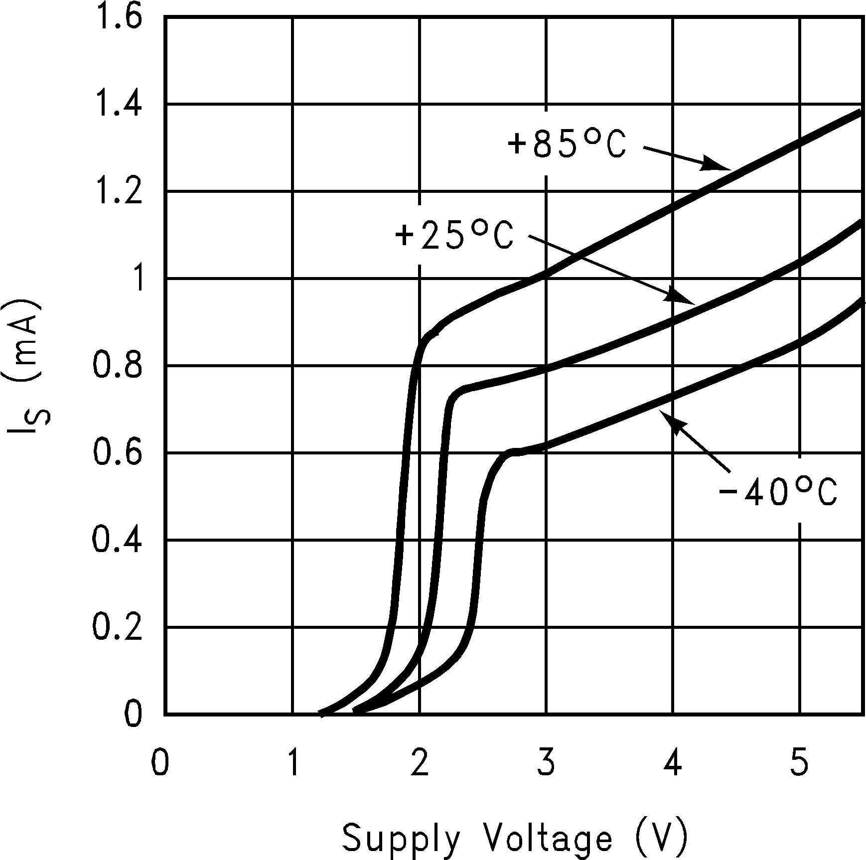
| VS = 5 V | ||
| VS = 5 V | ||
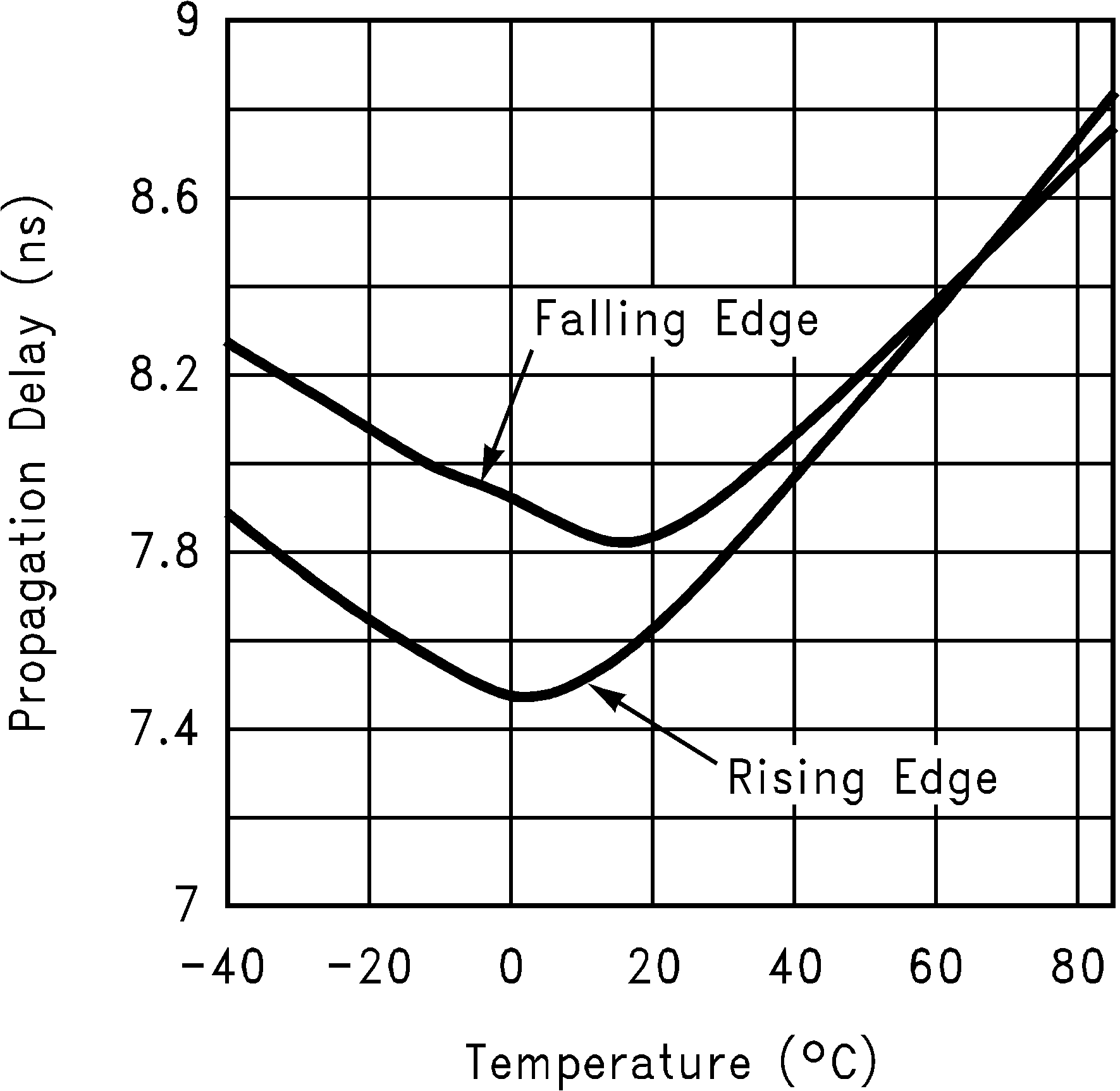
| VS = 5V | ||
| VOD = 15 mV | ||
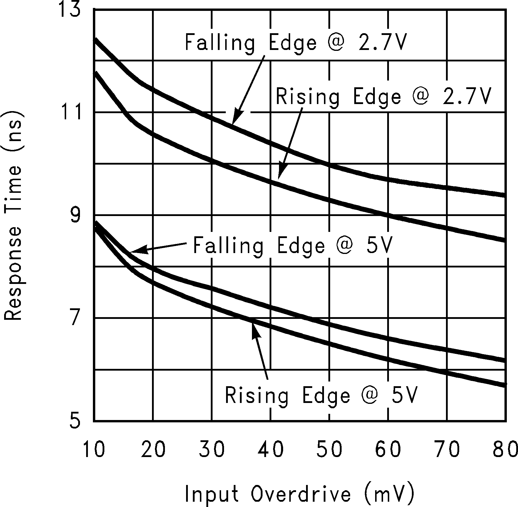
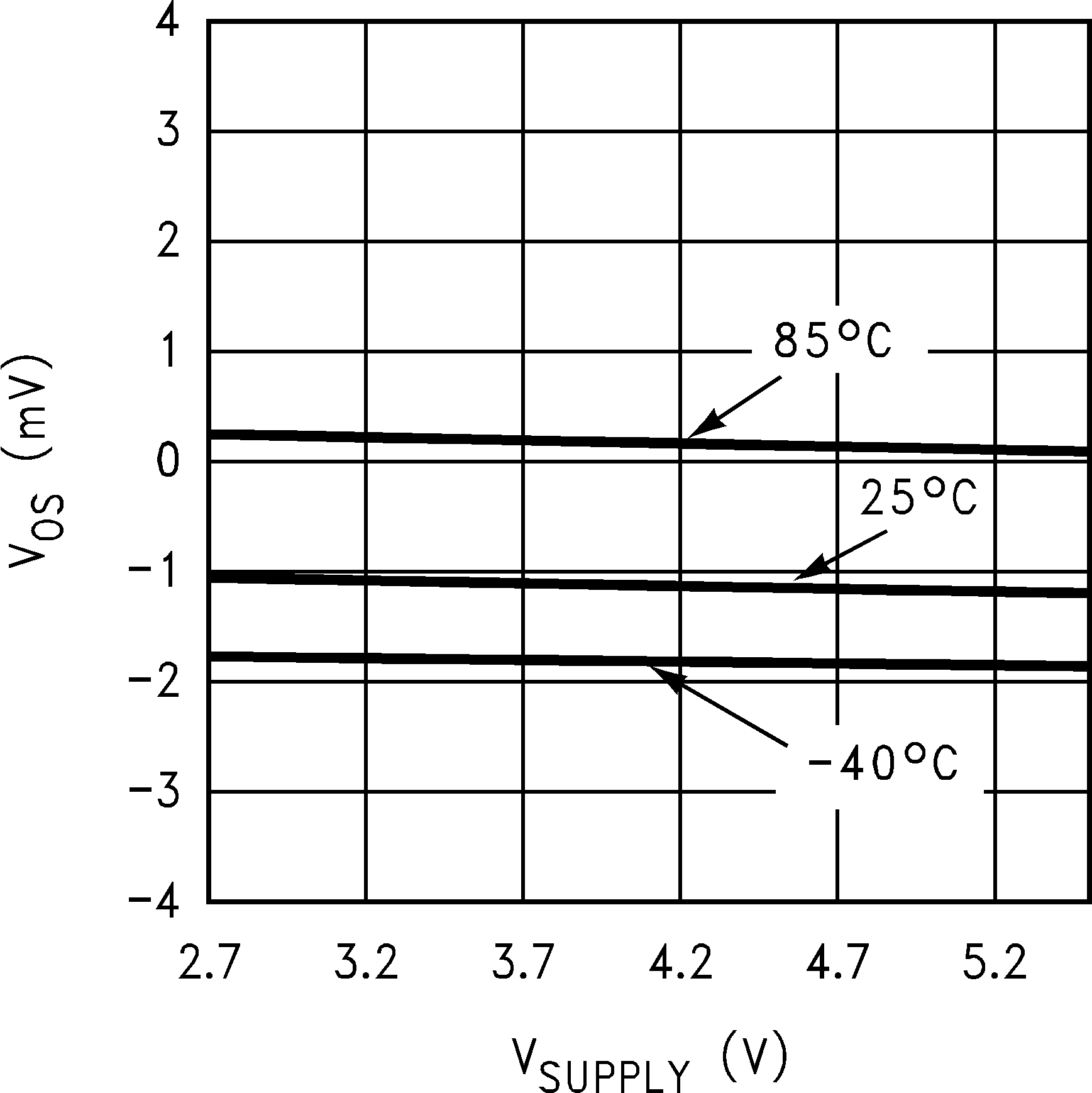
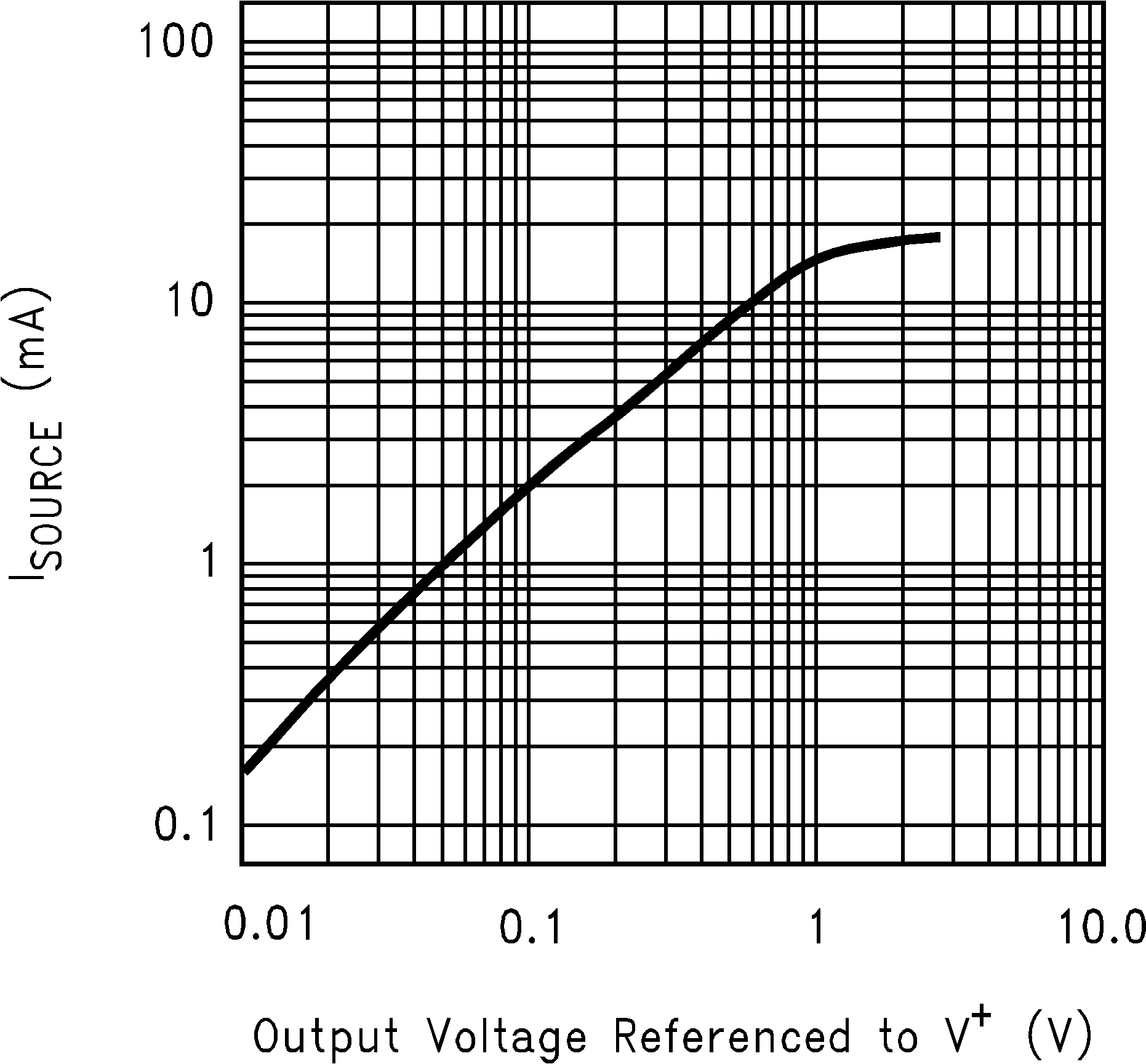
| VS = 2.7 V | ||
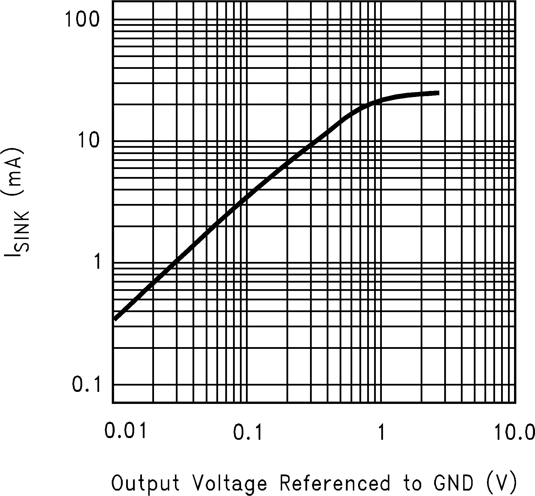
| VS = 2.7 V | ||
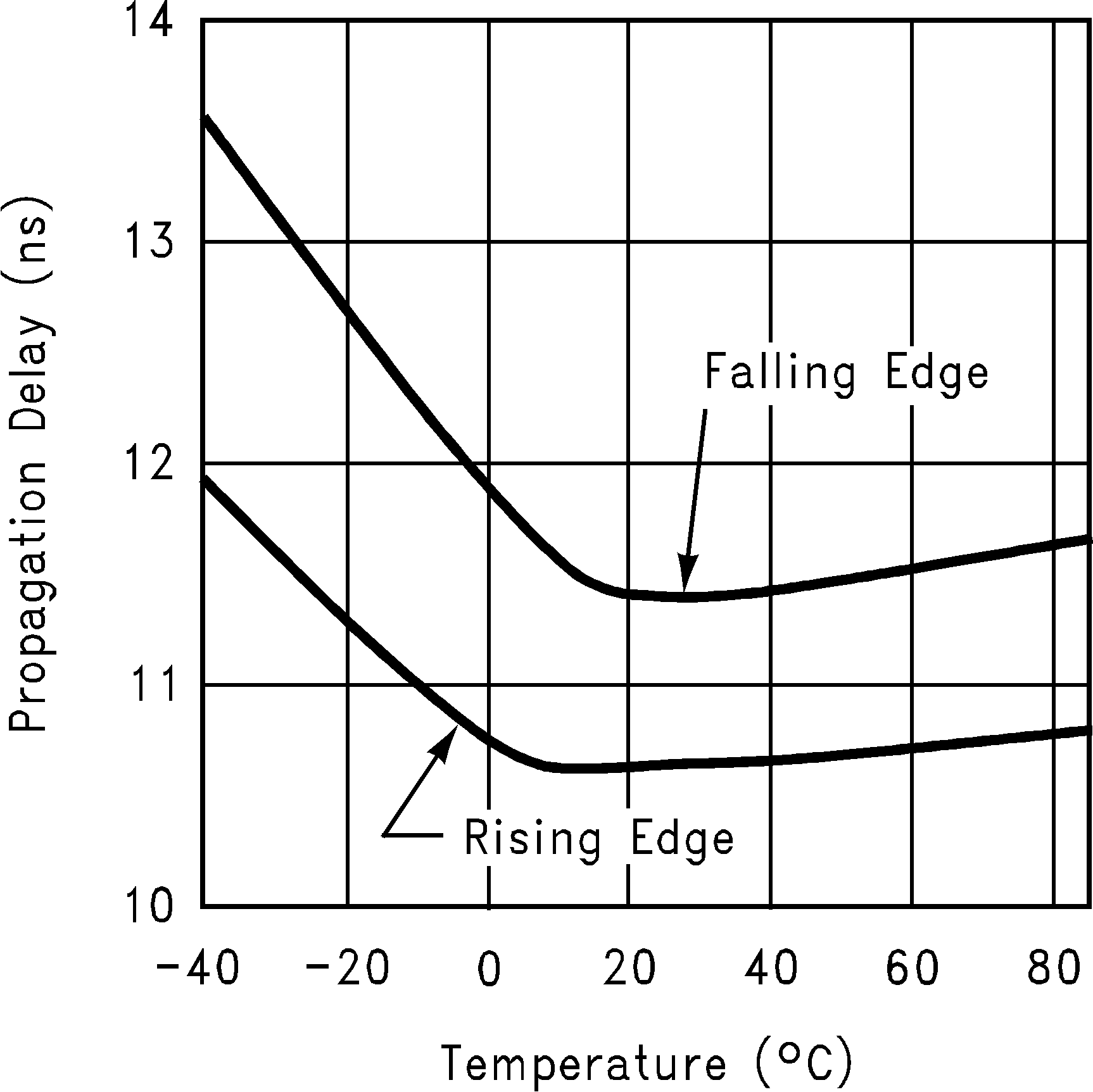
| VS = 2.7 V | ||
| VOD = 15 mV | ||
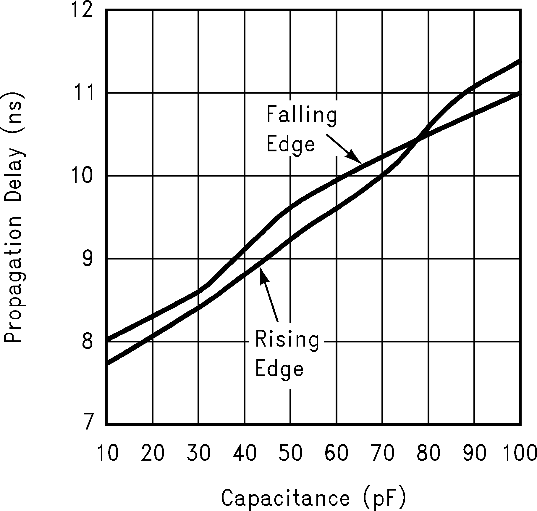
| VS = 5 V | ||
| VOD = 15 mV | ||
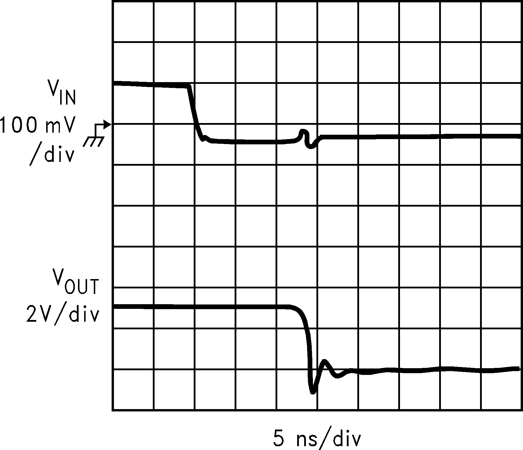
| VS = 2.7 V | ||
| CL = 10 pF | ||
| VOD = 15 mV |
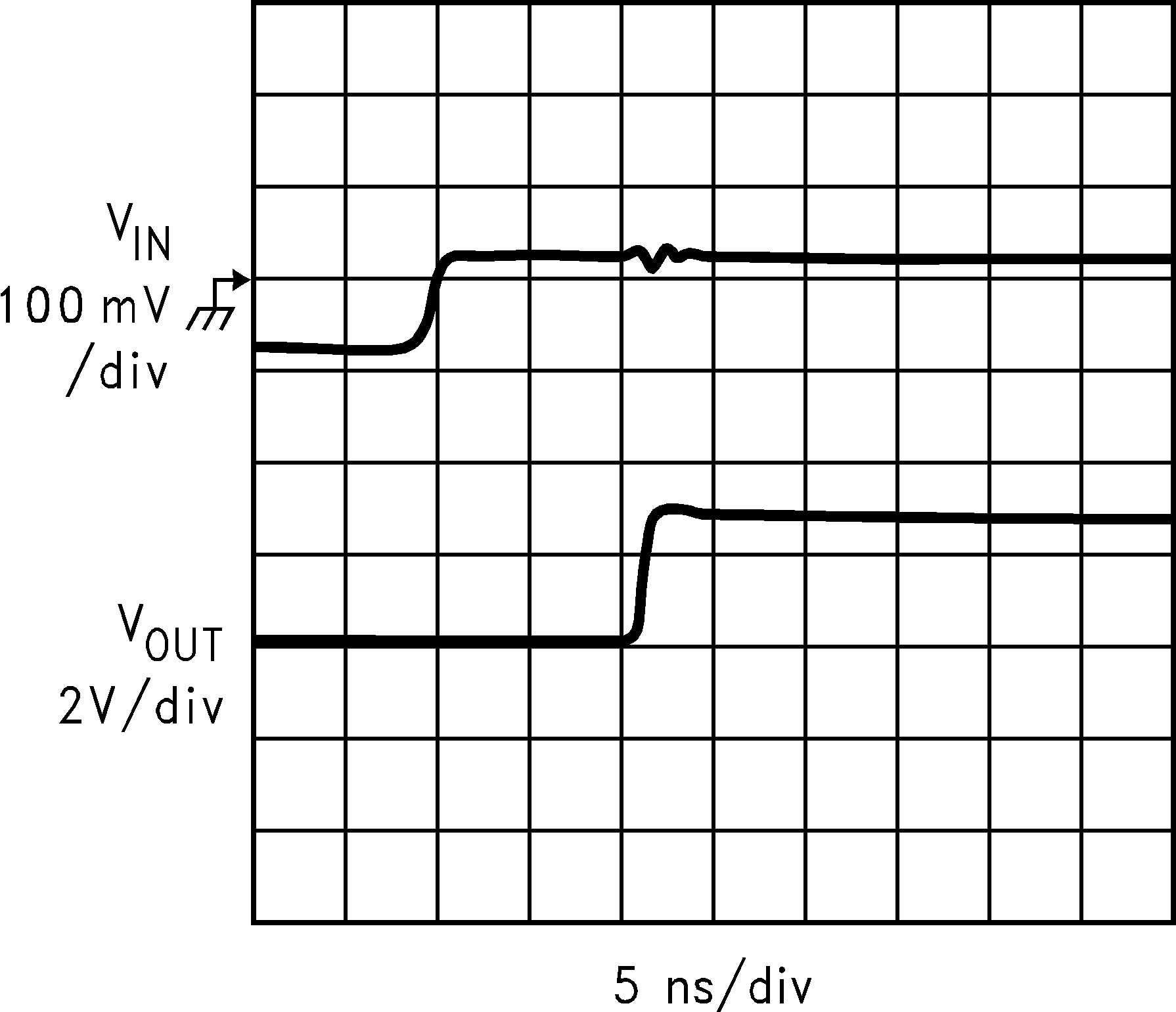
| VS = 2.7 V | ||
| CL = 10 pF | ||
| VOD = 15 mV |