ZHCSE14D June 2015 – June 2018 LMT01
PRODUCTION DATA.
- 1 特性
- 2 应用
- 3 说明
- 4 修订历史记录
- 5 Pin Configuration and Functions
-
6 Specifications
- 6.1 Absolute Maximum Ratings
- 6.2 ESD Ratings
- 6.3 Recommended Operating Conditions
- 6.4 Thermal Information
- 6.5 Electrical Characteristics
- 6.6 Electrical Characteristics - TO-92/LPG Pulse Count to Temperature LUT
- 6.7 Electrical Characteristics - WSON/DQX Pulse Count to Temperature LUT
- 6.8 Switching Characteristics
- 6.9 Timing Diagram
- 6.10 Typical Characteristics
- 7 Detailed Description
- 8 Application and Implementation
- 9 Power Supply Recommendations
- 10Layout
- 11器件和文档支持
- 12机械、封装和可订购信息
封装选项
机械数据 (封装 | 引脚)
散热焊盘机械数据 (封装 | 引脚)
- DQX|2
订购信息
8.3 System Examples
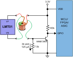
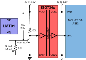
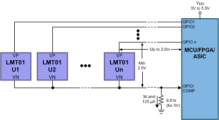
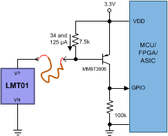
The LMT01 device can be configured in a number of ways. Transistor level shifting can be used so that the output pulse of the device can be read with a GPIO (see Figure 32). An isolation block can be inserted to achieve electrical isolation (see Figure 33). Multiple LMT01 devices can be controlled with GPIOs enabling temperature monitor for multiple zones. Lastly, the LMT01 device can be configured to have a common ground with a high side signal (see Figure 35).
 Figure 32. Transistor Level Shifting
 Figure 33. Isolation

Note: to turn off an LMT01 set the GPIO pin connected to VP to high impedance state as setting it low would cause the off LMT01 to be reverse biased. Comparator input of MCU must be used.
Figure 34. Connecting Multiple Devices to One MCU Input Pin

Note: the VN of the LMT01 must be connected to the MCU GND.
Figure 35. Common Ground With High-Side Signal