ZHCSF36A December 2015 – May 2016 LMR16010
PRODUCTION DATA.
- 1 特性
- 2 应用范围
- 3 说明
- 4 修订历史记录
- 5 Pin Configuration and Functions
- 6 Specifications
-
7 Detailed Description
- 7.1 Overview
- 7.2 Functional Block Diagram
- 7.3
Feature Description
- 7.3.1 Fixed Frequency Peak Current Mode Control
- 7.3.2 Slope Compensation
- 7.3.3 Sleep-mode
- 7.3.4 Low Dropout Operation and Bootstrap Voltage (BOOT)
- 7.3.5 Adjustable Output Voltage
- 7.3.6 Enable and Adjustable Under-voltage Lockout
- 7.3.7 Switching Frequency and Synchronization (RT/SYNC)
- 7.3.8 Power Good (PGOOD)
- 7.3.9 Over Current and Short Circuit Protection
- 7.3.10 Overvoltage Protection
- 7.3.11 Thermal Shutdown
- 7.4 Device Functional Modes
- 8 Application and Implementation
- 9 Power Supply Recommendations
- 10Layout
- 11器件和文档支持
- 12机械、封装和可订购信息
7 Detailed Description
7.1 Overview
The LMR16010 SIMPLE SWITCHER® regulator is an easy to use step-down DC-DC converter that operates from a 4.3 V to 60 V supply voltage. It integrates a 155 mΩ (typical) high-side MOSFET, and is capable of delivering up to 1 A DC load current with exceptional efficiency and thermal performance in a very small solution size. The operating current is typically 40 μA under no load condition (not switching). When the device is disabled, the supply current is typically 1 μA. An extended family is available in 2 A and 3 A load options in pin to pin compatible packages.
The LMR16010 implements constant frequency peak current mode control with Sleep-mode at light load to achieve high efficiency. The device is internally compensated, which reduces design time, and requires fewer external components. The switching frequency is programmable from 200 kHz to 2.5 MHz by an external resistor RT. The LMR16010 is also capable of synchronization to an external clock within the 250 kHz to 2.3 MHz frequency range, which allows the device to be optimized to fit small board space at higher frequency, or high efficient power conversion at lower frequency.
Other features are included for more comprehensive system requirements, including precision enable, and approximate 97% duty cycle by BOOT capacitor recharge circuit. These features provide a flexible and easy to use platform for a wide range of applications. Protection features include over temperature shutdown, VOUT over voltage protection (OVP), VIN under-voltage lockout (UVLO), cycle-by-cycle current limit, and short-circuit protection with frequency fold-back.
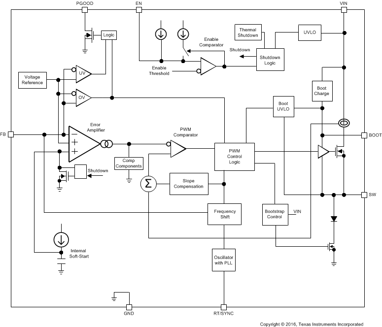
7.2 Functional Block Diagram
7.3 Feature Description
7.3.1 Fixed Frequency Peak Current Mode Control
The following operating description of the LMR16010 will refer to the Functional Block Diagram and to the waveforms in Figure 13. LMR16010 output voltage is regulated by turning on the high-side N-MOSFET with controlled ON time. During high-side switch ON time, the SW pin voltage swings up to approximately VIN, and the inductor current iL increase with linear slope (VIN – VOUT) / L. When high-side switch is off, inductor current discharges through freewheel diode with a slope of –VOUT / L. The control parameter of Buck converter is defined as Duty Cycle D = tON / TSW, where tON is the high-side switch ON time and TSW is the switching period. The regulator control loop maintains a constant output voltage by adjusting the duty cycle D. In an ideal Buck converter, where losses are ignored, D is proportional to the output voltage and inversely proportional to the input voltage: D = VOUT / VIN.
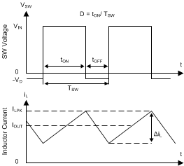 Figure 13. SW Node and Inductor Current Waveforms in
 Continuous Conduction Mode (CCM)
The LMR16010 employs fixed frequency peak current mode control. A voltage feedback loop is used to get accurate DC voltage regulation by adjusting the peak current command based on voltage offset. The peak inductor current is sensed from the high-side switch and compared to the peak current to control the ON time of the high-side switch. The voltage feedback loop is internally compensated, which allows for fewer external components, makes it easy to design, and provides stable operation with almost any combination of output capacitors. The regulator operates with fixed switching frequency at normal load condition. At very light load, the LMR16010 will operate in Sleep-mode to maintain high efficiency and the switching frequency will decrease with reduced load current.
7.3.2 Slope Compensation
The LMR16010 adds a compensating ramp to the MOSFET switch current sense signal. This slope compensation prevents sub-harmonic oscillations at duty cycles greater than 50%. The peak current limit of the high-side switch is not affected by the slope compensation and remains constant over the full duty cycle range.
7.3.3 Sleep-mode
The LMR16010 operates in Sleep-mode at light load currents to improve efficiency by reducing switching and gate drive losses. If the output voltage is within regulation and the peak switch current at the end of any switching cycle is below the current threshold of 300 mA, the device enters Sleep-mode. The Sleep-mode current threshold is the peak switch current level corresponding to a nominal internal COMP voltage of 400 mV.
When in Sleep-mode, the internal COMP voltage is clamped at 400 mV and the high-side MOSFET is inhibited, and the device draws only 40 μA (typical) input quiescent current. Since the device is not switching, the output voltage begins to decay. The voltage control loop responds to the falling output voltage by increasing the internal COMP voltage. The high-side MOSFET is enabled and switching resumes when the error amplifier lifts internal COMP voltage above 400 mV. The output voltage recovers to the regulated value, and internal COMP voltage eventually falls below the Sleep-mode threshold at which time the device again enters Sleep-mode.
7.3.4 Low Dropout Operation and Bootstrap Voltage (BOOT)
The LMR16010 provides an integrated bootstrap voltage regulator. A small capacitor between the BOOT and SW pins provides the gate drive voltage for the high-side MOSFET. The BOOT capacitor is refreshed when the high-side MOSFET is off and the external low side diode conducts. The recommended value of the BOOT capacitor is 0.1 μF. A ceramic capacitor with an X7R or X5R grade dielectric with a voltage rating of 16 V or greater is recommended for stable performance over temperature and voltage.
When operating with a low voltage difference from input to output, the high-side MOSFET of the LMR16010 will operate at approximate 97% duty cycle. When the high-side MOSFET is continuously on for 5 or 6 switching cycles (5 or 6 switching cycles for frequency lower than 1 MHz, and 10 or 11 switching cycles for frequency higher than 1 MHz) and the voltage from BOOT to SW drops below 3.2 V, the high-side MOSFET is turned off and an integrated low side MOSFET pulls SW low to recharge the BOOT capacitor.
Since the gate drive current sourced from the BOOT capacitor is small, the high-side MOSFET can remain on for many switching cycles before the MOSFET is turned off to refresh the capacitor. Thus the effective duty cycle of the switching regulator can be high, approaching 97%. The effective duty cycle of the converter during dropout is mainly influenced by the voltage drops across the power MOSFET, the inductor resistance, the low side diode voltage and the printed circuit board resistance.
7.3.5 Adjustable Output Voltage
The internal voltage reference produces a precise 0.75 V (typical) voltage reference over the operating temperature range. The output voltage is set by a resistor divider from output voltage to the FB pin. It is recommended to use 1% tolerance or better and temperature coefficient of 100 ppm or less divider resistors. Select the low side resistor RFBB for the desired divider current and use Equation 1 to calculate high-side RFBT. Larger value divider resistors are good for efficiency at light load. However, if the values are too high, the regulator will be more susceptible to noise and voltage errors from the FB input current may become noticeable. RFBB in the range from 10 kΩ to 100 kΩ is recommended for most applications.
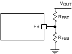 Figure 14. Output Voltage Setting

7.3.6 Enable and Adjustable Under-voltage Lockout
The LMR16010 is enabled when the VIN pin voltage rises above 4.0 V (typical) and the EN pin voltage exceeds the enable threshold of 1.2 V (typical). The LMR16010 is disabled when the VIN pin voltage falls below 3.715 V (typical) or when the EN pin voltage is below 1.2 V (typical). The EN pin has an internal pull-up current source (typically IEN = 1 μA) that enables operation of the LMR16010 when the EN pin is floating.
Many applications will benefit from the employment of an enable divider RENT and RENB in Figure 15 to establish a precision system UVLO level for the stage. System UVLO can be used for supplies operating from utility power as well as battery power. It can be used for sequencing, ensuring reliable operation, or supply protection, such as a battery. An external logic signal can also be used to drive EN input for system sequencing and protection.
When EN terminal voltage exceeds 1.2 V, an additional hysteresis current (typically IHYS = 3.6 μA) is sourced out of EN terminal. When the EN terminal is pulled below 1.2 V, IHYS current is removed. This additional current facilitates adjustable input voltage UVLO hysteresis. Use Equation 2 and Equation 3 to calculate RENT and RENB for desired UVLO hysteresis voltage.
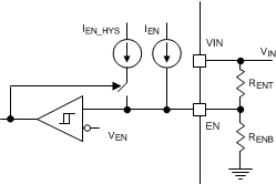 Figure 15. System UVLO By Enable Dividers


where VSTART is the desired voltage threshold to enable LMR16010, VSTOP is the desired voltage threshold to disable device, IEN = 1 μA and IHYS = 3.6 μA typically.
7.3.7 Switching Frequency and Synchronization (RT/SYNC)
The switching frequency of the LMR16010 can be programmed by the resistor RT from the RT/SYNC pin and GND pin. The RT/SYNC pin can’t be left floating or shorted to ground. To determine the timing resistance for a given switching frequency, use Equation 4 or the curve in Figure 16. Table 1 gives typical RT values for a given fSW.

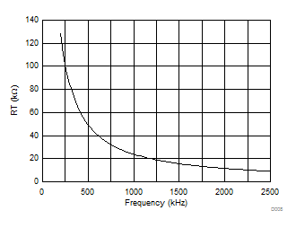 Figure 16. RT vs Frequency Curve
Table 1. Typical Frequency Setting RT Resistance
| fSW (kHz) | RT (kΩ) |
|---|---|
| 200 | 133 |
| 350 | 73.2 |
| 500 | 49.9 |
| 750 | 32.4 |
| 1000 | 23.2 |
| 1500 | 15.0 |
| 1912 | 11.5 |
| 2200 | 9.76 |
The LMR16010 switching action can also be synchronized to an external clock from 250 kHz to 2.3 MHz. Connect a square wave to the RT/SYNC pin through either circuit network shown in Figure 17. Internal oscillator is synchronized by the falling edge of external clock. The recommendations for the external clock include: high level no lower than 1.7 V, low level no higher than 0.5 V and have a pulse width greater than 30 ns. When using a low impedance signal source, the frequency setting resistor RT is connected in parallel with an AC coupling capacitor CCOUP to a termination resistor RTERM (e.g., 50 Ω). The two resistors in series provide the default frequency setting resistance when the signal source is turned off. A 10 pF ceramic capacitor can be used for CCOUP. Figure 18, Figure 19 and Figure 20 show the device synchronized to an external system clock.
 Figure 17. Synchronizing to an External Clock
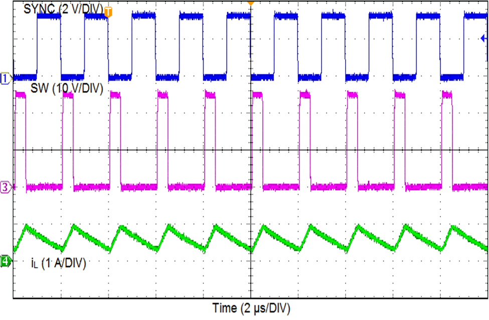 Figure 18. Synchronizing in CCM
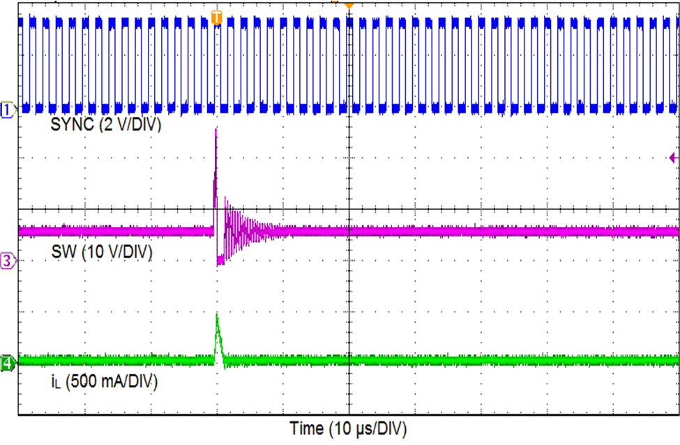 Figure 20. Synchronizing in Sleep-mode Mode
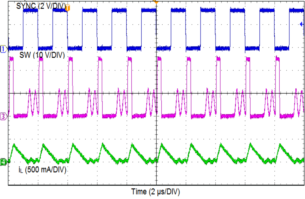 Figure 19. Synchronizing in DCM
Equation 5 calculates the maximum switching frequency limitation set by the minimum controllable on time and the input to output step down ratio. Setting the switching frequency above this value will cause the regulator to skip switching pulses to achieve the low duty cycle required at maximum input voltage.

where
- IOUT = Output current
- RIND = Inductor series resistance
- VIN_MAX = Maximum input voltage
- VOUT = Output voltage
- VD = Diode voltage drop
- RDS_ON = High-side MOSFET switch on resistance
- tON = Minimum on time
7.3.8 Power Good (PGOOD)
The LMR16010 has a built in power-good flag shown on PGOOD pin to indicate whether the output voltage is within its regulation level. The PGOOD signal can be used for start-up sequencing of multiple rails or fault protection. The PGOOD pin is an open-drain output that requires a pull-up resistor to an appropriate DC voltage. Voltage seen by the PGOOD pin should never exceed 7 V. A resistor divider pair can be used to divide the voltage down from a higher potential. A typical range of pull-up resistor value is 10 kΩ to 100 kΩ.
Refer to Figure 21. When the FB voltage is within the power-good band, +7% above and -6% below the internal reference VREF typically, the PGOOD switch will be turned off and the PGOOD voltage will be pulled up to the voltage level defined by the pull-up resistor or divider. When the FB voltage is outside of the tolerance band, +9% above or -8% below VREF typically, the PGOOD switch will be turned on and the PGOOD pin voltage will be pulled low to indicate power bad.
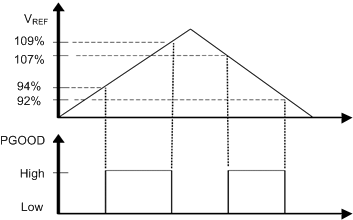 Figure 21. Power-Good Flag
7.3.9 Over Current and Short Circuit Protection
The LMR16010 is protected from over current condition by cycle-by-cycle current limiting on the peak current of the high-side MOSFET. High-side MOSFET over-current protection is implemented by the nature of the Peak Current Mode control. The high-side switch current is compared to the output of the Error Amplifier (EA) minus slope compensation every switching cycle. Please refer to Functional Block Diagram for more details. The peak current of high-side switch is limited by a clamped maximum peak current threshold which is constant. So the peak current limit of the high-side switch is not affected by the slope compensation and remains constant over the full duty cycle range.
The LMR16010 also implements a frequency fold-back to protect the converter in severe over-current or short conditions. The oscillator frequency is divided by 2, 4, and 8 as the FB pin voltage decrease to 75%, 50%, 25% of VREF. The frequency fold-back increases the off time by increasing the period of the switching cycle, so that it provides more time for the inductor current to ramp down and leads to a lower average inductor current. Lower frequency also means lower switching loss. Frequency fold-back reduces power dissipation and prevents overheating and potential damage to the device.
7.3.10 Overvoltage Protection
The LMR16010 employs an output overvoltage protection (OVP) circuit to minimize voltage overshoot when recovering from output fault conditions or strong unload transients in designs with low output capacitance. The OVP feature minimizes output overshoot by turning off high-side switch immediately when FB voltage reaches to the rising OVP threshold which is nominally 109% of the internal voltage reference VREF. When the FB voltage drops below the falling OVP threshold which is nominally 107% of VREF, the high-side MOSFET resumes normal operation.
7.3.11 Thermal Shutdown
The LMR16010 provides an internal thermal shutdown to protect the device when the junction temperature exceeds 170 °C (typical). The high-side MOSFET stops switching when thermal shundown activates. Once the die temperature falls below 158 °C (typical), the device reinitiates the power up sequence controlled by the internal soft-start circuitry.
7.4 Device Functional Modes
7.4.1 Shutdown Mode
The EN pin provides electrical ON and OFF control for the LMR16010. When VEN is below 1.0 V, the device is in shutdown mode. The switching regulator is turned off and the quiescent current drops to 1.0 µA typically. The LMR16010 also employs under voltage lock out protection. If VIN voltage is below the UVLO level, the regulator will be turned off.
7.4.2 Active Mode
The LMR16010 is in Active Mode when VEN is above the precision enable threshold and VIN is above its UVLO level. The simplest way to enable the LMR16010 is to connect the EN pin to VIN pin. This allows self startup when the input voltage is in the operation range: 4.3 V to 60 V. Please refer to Enable and Adjustable Under-voltage Lockout for details on setting these operating levels.
In Active Mode, depending on the load current, the LMR16010 will be in one of three modes:
- Continuous conduction mode (CCM) with fixed switching frequency when load current is above half of the peak-to-peak inductor current ripple.
- Discontinuous conduction mode (DCM) with fixed switching frequency when load current is lower than half of the peak-to-peak inductor current ripple in CCM operation.
- Sleep-mode when internal COMP voltage drop to 400 mV at very light load.
7.4.3 CCM Mode
CCM operation is employed in the LMR16010 when the load current is higher than half of the peak-to-peak inductor current. In CCM operation, the frequency of operation is fixed, output voltage ripple will be at a minimum in this mode and the maximum output current of 1 A can be supplied by the LMR16010.
7.4.4 Light Load Operation
When the load current is lower than half of the peak-to-peak inductor current in CCM, the LMR16010 will operate in DCM. At even lighter current loads, Sleep-mode is activated to maintain high efficiency operation by reducing switching and gate drive losses.