ZHCSA20C October 2011 – June 2019 LMR10510
PRODUCTION DATA.
- 1 特性
- 2 应用
- 3 说明
- 4 修订历史记录
- 5 说明(续)
- 6 Pin Configuration and Functions
- 7 Specifications
- 8 Detailed Description
- 9 Application and Implementation
- 10Layout
- 11器件和文档支持
- 12机械、封装和可订购信息
8.1 Overview
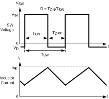
The following operating description of the LMR10510 refers to Functional Block Diagram and to the waveforms in Figure 14. The LMR10510 supplies a regulated output voltage by switching the internal PMOS control switch at constant frequency and variable duty cycle. A switching cycle begins at the falling edge of the reset pulse generated by the internal oscillator. When this pulse goes low, the output control logic turns on the internal PMOS control switch. During this on-time, the SW pin voltage (VSW) swings up to approximately VIN, and the inductor current (IL) increases with a linear slope. IL is measured by the current sense amplifier, which generates an output proportional to the switch current. The sense signal is summed with the regulator’s corrective ramp and compared to the error amplifier’s output, which is proportional to the difference between the feedback voltage and VREF. When the PWM comparator output goes high, the output switch turns off until the next switching cycle begins. During the switch off-time, inductor current discharges through the Schottky catch diode, which forces the SW pin to swing below ground by the forward voltage (VD) of the Schottky catch diode. The regulator loop adjusts the duty cycle (D) to maintain a constant output voltage.
 Figure 14. Typical Waveforms