ZHCSQG1H November   2009  – May 2022 LMP8645 , LMP8645HV

PRODUCTION DATA  

  1. 特性
  2. 应用
  3. 说明
  4. Revision History
  5. Pin Configuration and Functions
  6. Specifications
    1. 6.1 Absolute Maximum Ratings
    2. 6.2 ESD Ratings
    3. 6.3 Recommended Operating Conditions
    4. 6.4 Thermal Information
    5. 6.5 2.7-V Electrical Characteristics
    6. 6.6 5-V Electrical Characteristics
    7. 6.7 12-V Electrical Characteristics
    8. 6.8 Typical Characteristics
  7. Detailed Description
    1. 7.1 Overview
      1. 7.1.1 Theory of Operation
    2. 7.2 Functional Block Diagram
    3. 7.3 Feature Description
      1. 7.3.1 Driving ADC
      2. 7.3.2 Applying Input Voltage With No Supply Voltage
    4. 7.4 Device Functional Modes
      1. 7.4.1 Selection of the Gain Resistor
      2. 7.4.2 Gain Range Limitations
        1. 7.4.2.1 Range 1: VCM is –2 V to 1.8 V
        2. 7.4.2.2 Range 2: VCM is 1.8 V to VS
        3. 7.4.2.3 Range 3: VCM is greater than VS
      3. 7.4.3 Selection of Sense Resistor
        1. 7.4.3.1 Resistor Power Rating and Thermal Issues
        2. 7.4.3.2 Using PCB Trace as a Sense Resistor
      4. 7.4.4 Sense Line Inputs
        1. 7.4.4.1 Effects of Series Resistance on Sense Lines
  8. Application and Implementation
    1. 8.1 Application Information
    2. 8.2 Typical Applications
      1. 8.2.1 Typical Current Monitor Application
        1. 8.2.1.1 Design Requirements
        2. 8.2.1.2 Detailed Design Procedure
        3. 8.2.1.3 Application Curves
      2. 8.2.2 High Brightness LED Driver
  9. Power Supply Recommendations
  10. 10Layout
    1. 10.1 Layout Guidelines
    2. 10.2 Layout Example
  11. 11Device and Documentation Support
    1. 11.1 Device Support
      1. 11.1.1 Development Support
    2. 11.2 Documentation Support
      1. 11.2.1 Related Documentation
    3. 11.3 接收文档更新通知
    4. 11.4 支持资源
    5. 11.5 Trademarks
    6. 11.6 Electrostatic Discharge Caution
    7. 11.7 术语表
  12. 12Mechanical, Packaging, and Orderable Information

封装选项

机械数据 (封装 | 引脚)
散热焊盘机械数据 (封装 | 引脚)
订购信息

Range 1: VCM is –2 V to 1.8 V

The maximum voltage at the RG pin is given by the following inequality:

Equation 4. VRG = Vsense × RGAIN × Gm ≤ min (1.3 V; Vout_max)

where

  • Vout_max is the maximum allowable output voltage according to the Electrical Tables

All the gain resistors (RGAIN) values which respect the previous inequality are allowed. The graphical representation of Figure 7-3 helps in the selection.

All the combinations (VSENSE , RGAIN) below the curve are allowed.
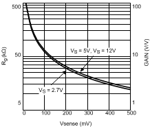
GUID-84B467B1-735B-421D-9608-0757C26D1BC3-low.gifFigure 7-3 Allowed Gains for Range 1

As a consequence, once selected, the gain (RGAIN) and the VSENSE range is fixed, too.

For example if an application required a Gain of 10, RG will be 50 kΩ and VSENSE will be in the range 10 mV to 100 mV.