ZHCSID6A December   2018  – December 2018 LMK05318

PRODUCTION DATA.  

  1. 特性
  2. 应用
  3. 说明
    1.     Device Images
      1.      简化方框图
  4. 修订历史记录
  5. (说明 (续))
  6. Pin Configuration and Functions
    1.     Pin Functions
    2. 6.1 Device Start-Up Modes
  7. Specifications
    1. 7.1 Absolute Maximum Ratings
    2. 7.2 ESD Ratings
    3. 7.3 Recommended Operating Conditions
    4. 7.4 Thermal Information: 4-Layer JEDEC Standard PCB
    5. 7.5 Thermal Information: 10-Layer Custom PCB
    6. 7.6 Electrical Characteristics
    7. 7.7 Timing Diagrams
    8. 7.8 Typical Characteristics
  8. Parameter Measurement Information
    1. 8.1 Output Clock Test Configurations
  9. Detailed Description
    1. 9.1 Overview
      1. 9.1.1 ITU-T G.8262 (SyncE) Standards Compliance
    2. 9.2 Functional Block Diagram
      1. 9.2.1 PLL Architecture Overview
      2. 9.2.2 DPLL Mode
      3. 9.2.3 APLL-Only Mode
    3. 9.3 Feature Description
      1. 9.3.1  Oscillator Input (XO_P/N)
      2. 9.3.2  Reference Inputs (PRIREF_P/N and SECREF_P/N)
      3. 9.3.3  Clock Input Interfacing and Termination
      4. 9.3.4  Reference Input Mux Selection
        1. 9.3.4.1 Automatic Input Selection
        2. 9.3.4.2 Manual Input Selection
      5. 9.3.5  Hitless Switching
        1. 9.3.5.1 Hitless Switching With 1-PPS Inputs
      6. 9.3.6  Gapped Clock Support on Reference Inputs
      7. 9.3.7  Input Clock and PLL Monitoring, Status, and Interrupts
        1. 9.3.7.1 XO Input Monitoring
        2. 9.3.7.2 Reference Input Monitoring
          1. 9.3.7.2.1 Reference Validation Timer
          2. 9.3.7.2.2 Amplitude Monitor
          3. 9.3.7.2.3 Frequency Monitoring
          4. 9.3.7.2.4 Missing Pulse Monitor (Late Detect)
          5. 9.3.7.2.5 Runt Pulse Monitor (Early Detect)
          6. 9.3.7.2.6 Phase Valid Monitor for 1-PPS Inputs
        3. 9.3.7.3 PLL Lock Detectors
        4. 9.3.7.4 Tuning Word History
        5. 9.3.7.5 Status Outputs
        6. 9.3.7.6 Interrupt
      8. 9.3.8  PLL Relationships
        1. 9.3.8.1  PLL Frequency Relationships
        2. 9.3.8.2  Analog PLLs (APLL1, APLL2)
        3. 9.3.8.3  APLL Reference Paths
          1. 9.3.8.3.1 APLL XO Doubler
          2. 9.3.8.3.2 APLL1 XO Reference (R) Divider
          3. 9.3.8.3.3 APLL2 Reference (R) Dividers
        4. 9.3.8.4  APLL Phase Frequency Detector (PFD) and Charge Pump
        5. 9.3.8.5  APLL Feedback Divider Paths
          1. 9.3.8.5.1 APLL1 N Divider With SDM
          2. 9.3.8.5.2 APLL2 N Divider With SDM
        6. 9.3.8.6  APLL Loop Filters (LF1, LF2)
        7. 9.3.8.7  APLL Voltage Controlled Oscillators (VCO1, VCO2)
          1. 9.3.8.7.1 VCO Calibration
        8. 9.3.8.8  APLL VCO Clock Distribution Paths (P1, P2)
        9. 9.3.8.9  DPLL Reference (R) Divider Paths
        10. 9.3.8.10 DPLL Time-to-Digital Converter (TDC)
        11. 9.3.8.11 DPLL Loop Filter (DLF)
        12. 9.3.8.12 DPLL Feedback (FB) Divider Path
      9. 9.3.9  Output Clock Distribution
      10. 9.3.10 Output Channel Muxes
      11. 9.3.11 Output Dividers (OD)
      12. 9.3.12 Clock Outputs (OUTx_P/N)
        1. 9.3.12.1 AC-Differential Output (AC-DIFF)
        2. 9.3.12.2 HCSL Output
        3. 9.3.12.3 1.8-V LVCMOS Output
        4. 9.3.12.4 Output Auto-Mute During LOL
      13. 9.3.13 Glitchless Output Clock Start-Up
      14. 9.3.14 Clock Output Interfacing and Termination
      15. 9.3.15 Output Synchronization (SYNC)
      16. 9.3.16 Zero-Delay Mode (ZDM) Synchronization for 1-PPS Input and Output
    4. 9.4 Device Functional Modes
      1. 9.4.1 Device Start-Up Modes
        1. 9.4.1.1 EEPROM Mode
        2. 9.4.1.2 ROM Mode
      2. 9.4.2 PLL Operating Modes
        1. 9.4.2.1 Free-Run Mode
        2. 9.4.2.2 Lock Acquisition
        3. 9.4.2.3 Locked Mode
        4. 9.4.2.4 Holdover Mode
      3. 9.4.3 PLL Start-Up Sequence
      4. 9.4.4 Digitally-Controlled Oscillator (DCO) Mode
        1. 9.4.4.1 DCO Frequency Step Size
        2. 9.4.4.2 DCO Direct-Write Mode
      5. 9.4.5 Zero-Delay Mode Synchronization
    5. 9.5 Programming
      1. 9.5.1 Interface and Control
      2. 9.5.2 I2C Serial Interface
        1. 9.5.2.1 I2C Block Register Transfers
      3. 9.5.3 SPI Serial Interface
        1. 9.5.3.1 SPI Block Register Transfer
      4. 9.5.4 Register Map and EEPROM Map Generation
      5. 9.5.5 General Register Programming Sequence
      6. 9.5.6 EEPROM Programming Flow
        1. 9.5.6.1 EEPROM Programming Using Method #1 (Register Commit)
          1. 9.5.6.1.1 Write SRAM Using Register Commit
          2. 9.5.6.1.2 Program EEPROM
        2. 9.5.6.2 EEPROM Programming Using Method #2 (Direct Writes)
          1. 9.5.6.2.1 Write SRAM Using Direct Writes
          2. 9.5.6.2.2 User-Programmable Fields In EEPROM
      7. 9.5.7 Read SRAM
      8. 9.5.8 Read EEPROM
      9. 9.5.9 EEPROM Start-Up Mode Default Configuration
  10. 10Application and Implementation
    1. 10.1 Application Information
      1. 10.1.1 Device Start-Up Sequence
      2. 10.1.2 Power Down (PDN) Pin
      3. 10.1.3 Power Rail Sequencing, Power Supply Ramp Rate, and Mixing Supply Domains
        1. 10.1.3.1 Mixing Supplies
        2. 10.1.3.2 Power-On Reset (POR) Circuit
        3. 10.1.3.3 Powering Up From a Single-Supply Rail
        4. 10.1.3.4 Power Up From Split-Supply Rails
        5. 10.1.3.5 Non-Monotonic or Slow Power-Up Supply Ramp
      4. 10.1.4 Slow or Delayed XO Start-Up
    2. 10.2 Typical Application
      1. 10.2.1 Design Requirements
      2. 10.2.2 Detailed Design Procedure
      3. 10.2.3 Application Curves
    3. 10.3 Do's and Don'ts
  11. 11Power Supply Recommendations
    1. 11.1 Power Supply Bypassing
    2. 11.2 Device Current and Power Consumption
      1. 11.2.1 Current Consumption Calculations
      2. 11.2.2 Power Consumption Calculations
      3. 11.2.3 Example
  12. 12Layout
    1. 12.1 Layout Guidelines
    2. 12.2 Layout Example
    3. 12.3 Thermal Reliability
      1. 12.3.1 Support for PCB Temperature up to 105°C
  13. 13器件和文档支持
    1. 13.1 器件支持
      1. 13.1.1 TICS Pro
      2. 13.1.2 相关文档
    2. 13.2 接收文档更新通知
    3. 13.3 社区资源
    4. 13.4 商标
    5. 13.5 静电放电警告
    6. 13.6 术语表
  14. 14机械、封装和可订购信息

封装选项

请参考 PDF 数据表获取器件具体的封装图。

机械数据 (封装 | 引脚)
  • RGZ|48
散热焊盘机械数据 (封装 | 引脚)
订购信息

Reference Inputs (PRIREF_P/N and SECREF_P/N)

The reference inputs (PRIREF and SECREF) can accept differential or single-ended clocks. Each input has programmable input type, termination, and AC-coupled input biasing configurations as shown in Figure 28. Each input buffer drives the reference input mux of the DPLL block. The DPLL input mux can select from any of the reference inputs. The DPLL can switch between inputs with different frequencies provided they can be divided-down to a common frequency by DPLL R dividers. The reference input paths also drive the various detector blocks for reference input monitoring and validation.
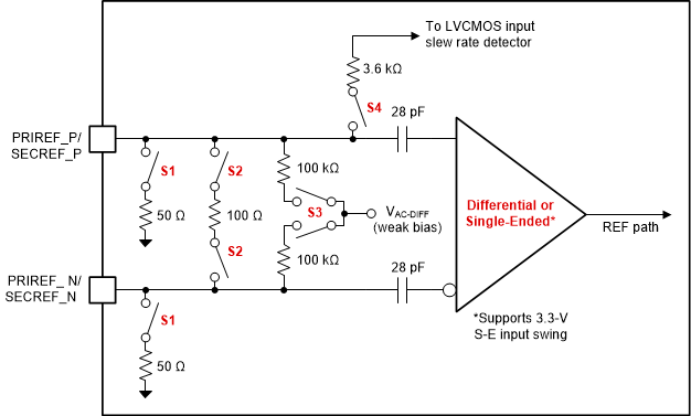
LMK05318 differential_input_buffer.gifFigure 28. Reference Input Buffer

Table 3 lists the reference input buffer configurations for common clock interface types.

Table 3. Reference Input Buffer Modes

REFx_TYPE INPUT TYPES INTERNAL SWITCH SETTINGS
INTERNAL TERM.
(S1, S2)(1)
INTERNAL BIAS
(S3)(2)
LVCMOS SLEW RATE DETECT (S4)(3)
0h LVDS, CML, LVPECL
(DC-coupled)
OFF OFF OFF
1h LVDS, CML, LVPECL
(AC-coupled)
OFF ON (1.3 V) OFF
3h LVDS, CML, LVPECL
(AC-coupled, internal 100-Ω)
100 Ω ON (1.3 V) OFF
4h HCSL
(DC-coupled, internal 50-Ω)
50 Ω OFF OFF
8h LVCMOS
(DC-coupled)
OFF OFF ON
Ch Single-ended
(DC-coupled, internal 50-Ω)
50 Ω OFF ON
S1, S2: OFF = External termination is assumed.
S3: OFF = External input bias or DC coupling is assumed.
S4: OFF = Differential input amplitude detector is used for all input types except LVCMOS or Single-ended.