SNOS986E December 2001 – July 2014 LMH6622
PRODUCTION DATA.
- 1 Features
- 2 Applications
- 3 Description
- 4 Revision History
- 5 Pin Configuration and Functions
- 6 Specifications
- 7 Parameter Measurement Information
- 8 Detailed Description
- 9 Application and Implementation
- 10Power Supply Recommendations
- 11Layout
- 12Device and Documentation Support
- 13Mechanical, Packaging, and Orderable Information
封装选项
机械数据 (封装 | 引脚)
散热焊盘机械数据 (封装 | 引脚)
- DGK|8
订购信息
6 Specifications
6.1 Absolute Maximum Ratings(1)(1)
| MIN | MAX | UNIT | ||
|---|---|---|---|---|
| VIN Differential | ±1.2 | V | ||
| Supply Voltage (V+ – V−) | 13.2 | V | ||
| Voltage at Input Pins | V+ +0.5, V− −0.5 | V | ||
| SOLDERING INFORMATION | ||||
| Infrared or Convection (20 sec) | 235 | °C | ||
| Wave Soldering (10 sec) | 260 | °C | ||
| Junction Temperature (4) | +150 | °C | ||
(1) If Military/Aerospace specified devices are required, please contact the Texas Instruments Sales Office/Distributors for availability and specifications.
6.2 Handling Ratings
| MIN | MAX | UNIT | |||
|---|---|---|---|---|---|
| Tstg | Storage temperature range | −65° | +150 | °C | |
| V(ESD) | Electrostatic discharge | Human body model (HBM), per ANSI/ESDA/JEDEC JS-001, all pins(1) | 2000(2) | V | |
| Charged device model (CDM), per JEDEC specification JESD22-C101, all pins(2) | 200(2) | ||||
(1) JEDEC document JEP155 states that 2000-V HBM allows safe manufacturing with a standard ESD control process.
(2) JEDEC document JEP157 states that 200-V CDM allows safe manufacturing with a standard ESD control process.
6.3 Recommended Operating Conditions(1)
| MIN | MAX | UNIT | ||
|---|---|---|---|---|
| Supply Voltage (V+– V−) | ±2.25 | ±6 | V | |
| Temperature Range(3)(4) | −40 | +85 | °C | |
(1) Absolute Maximum Ratings indicate limits beyond which damage to the device may occur. Operating Ratings indicate conditions for which the device is intended to be functional, but specific performance is not ensured. For ensured specifications and the test conditions, see the Electrical Characteristics.
6.4 Thermal Information
| THERMAL METRIC(1) | LMH6622 | LMH6622 | UNIT | |
|---|---|---|---|---|
| Package D | Package DGK | |||
| 8 PINS | 8 PINS | |||
| RθJA | Junction-to-ambient thermal resistance(4) | 166° | 211° | °C/W |
(1) For more information about traditional and new thermal metrics, see the IC Package Thermal Metrics application report, SPRA953.
6.5 ±6 V Electrical Characteristics
Unless otherwise specified, TJ = 25°C, V+ = 6 V, V− = −6 V, VCM = 0 V, AV = +2, RF = 500 Ω, RL = 100 Ω. Some limits apply at the temperature extremes as noted in the table.| PARAMETER | TEST CONDITIONS | TEMPERATURE EXTREMES |
ROOM TEMPERATURE |
UNIT | |||||
|---|---|---|---|---|---|---|---|---|---|
| MIN(6) | TYP(5) | MAX(6) | MIN(6) | TYP(5) | MAX(6) | ||||
| DYNAMIC PERFORMANCE | |||||||||
| fCL | −3dB BW | VO = 200 mVPP | 160 | MHz | |||||
| BW0.1dB | 0.1dB Gain Flatness | VO = 20 0mVPP | 30 | MHz | |||||
| SR | Slew Rate(8) | VO = 2 VPP | 85 | V/μs | |||||
| TS | Settling Time | VO = 2 VPP to ±0.1% | 40 | ns | |||||
| VO = 2 VPP to ±1.0% | 35 | ||||||||
| Tr | Rise Time | VO = 0.2 V Step, 10% to 90% | 2.3 | ns | |||||
| Tf | Fall Time | VO = 0.2 V Step, 10% to 90% | 2.3 | ns | |||||
| DISTORTION and NOISE RESPONSE | |||||||||
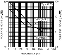
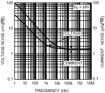
| en | Input Referred Voltage Noise | f = 100 kHz | 1.6 | nV/√Hz | |||||
| in | Input Referred Current Noise | f = 100 kHz | 1.5 | pA/√Hz | |||||
| DG | Differential Gain | RL = 150 Ω, RF = 470 Ω, NTSC | 0.03% | ||||||
| DP | Differential Phase | RL = 150 Ω, RF = 470 Ω, NTSC | 0.03 | deg | |||||
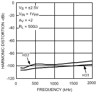
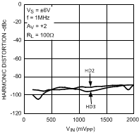
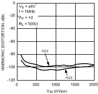
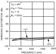
| HD2 | 2nd Harmonic Distortion | fc = 1 MHz, VO = 2 VPP, RL = 100 Ω |
−90 | dBc | |||||
| fc = 1 MHz, VO = 2 VPP, RL = 500 Ω |
−100 | ||||||||
| HD3 | 3rd Harmonic Distortion | fc = 1 MHz, VO = 2 VPP, RL = 100 Ω |
−94 | dBc | |||||
| fc = 1 MHz, VO = 2 VPP, RL = 500 Ω |
−100 | ||||||||
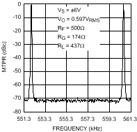
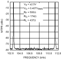
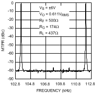
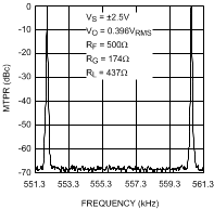
| MTPR | Upstream | VO = 0.6 VRMS, 26 kHz to 132 kHz (see Figure 33) |
−78 | dBc | |||||
| Downstream | VO = 0.6 VRMS, 144 kHz to 1.1 MHz (see Figure 33) |
−70 | |||||||
| INPUT CHARACTERISTICS | |||||||||
| VOS | Input Offset Voltage | VCM = 0 V | −2 | +2 | −1.2 | +0.2 | +1.2 | mV | |
| TC VOS | Input Offset Average Drift | VCM = 0 V(7) | −2.5 | μV/°C | |||||
| IOS | Input Offset Current | VCM = 0V | −1.5 | 1.5 | −1 | −0.04 | 1 | μA | |
| IB | Input Bias Current | VCM = 0V | 15 | 4.7 | 10 | μA | |||
| RIN | Input Resistance | Common Mode | 17 | MΩ | |||||
| Differential Mode | 12 | kΩ | |||||||
| CIN | Input Capacitance | Common Mode | 0.9 | pF | |||||
| Differential Mode | 1.0 | pF | |||||||
| CMVR | Input Common Mode Voltage Range | CMRR ≥ 60dB | −4.75 | −4.5 | V | ||||
| 5.5 | +5.7 | ||||||||
| CMRR | Common-Mode Rejection Ratio | Input Referred, VCM = −4.2 V to +5.2 V |
75 | 80 | 100 | dB | |||
| TRANSFER CHARACTERISTICS | |||||||||
| AVOL | Large Signal Voltage Gain | VO = 4 VPP | 70 | 74 | 83 | dB | |||
| Xt | Crosstalk | f = 1 MHz | −75 | dB | |||||
| OUTPUT CHARACTERISTICS | |||||||||
| VO | Output Swing | No Load, Positive Swing | 4.6 | 4.8 | 5.2 | V | |||
| No Load, Negative Swing | −4.4 | −5.0 | −4.6 | ||||||
| RL = 100 Ω, Positive Swing | 3.8 | 4.0 | 4.6 | ||||||
| RL = 100 Ω, Negative Swing | −3.8 | −4.6 | −4 | ||||||
| RO | Output Impedance | f = 1 MHz | 0.08 | Ω | |||||
| ISC | Output Short Circuit Current | Sourcing to Ground ΔVIN = 200 mV(3),(9) |
100 | 135 | mA | ||||
| Sinking to Ground ΔVIN = −200 mV(3),(9) |
100 | 130 | |||||||
| IOUT | Output Current | Sourcing, VO = +4.3 V Sinking, VO = −4.3 V |
90 | mA | |||||
| POWER SUPPLY | |||||||||
| +PSRR | Positive Power Supply Rejection Ratio |
Input Referred, VS = +5 V to +6 V |
74 | 80 | 95 | dB | |||
| −PSRR | Negative Power Supply Rejection Ratio | Input Referred, VS = −5 V to −6 V |
69 | 75 | 90 | ||||
| IS | Supply Current (per amplifier) | No Load | 6.5 | 4.3 | 6 | mA | |||
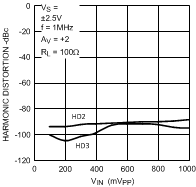
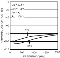
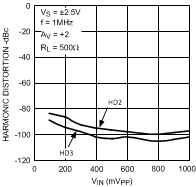
6.6 ±2.5 V Electrical Characteristics
Unless otherwise specified, TJ = 25°C, V+ = 2.5 V, V− = −2.5 V, VCM = 0 V, AV = +2, RF = 500 Ω, RL = 100 Ω. Some limits apply at the temperature extremes as noted in the table.| PARAMETER | TEST CONDITIONS | TEMPERATURE EXTREMES |
ROOM TEMPERATURE |
UNIT | |||||
|---|---|---|---|---|---|---|---|---|---|
| MIN(6) | TYP(5) | MAX(6) | MIN(6) | TYP(5) | MAX(6) | ||||
| DYNAMIC PERFORMANCE | |||||||||
| fCL | −3 dB BW | VO = 200 mVPP | 150 | MHz | |||||
| BW0.1dB | 0.1dB Gain Flatness | VO = 200 mVPP | 20 | MHz | |||||
| SR | Slew Rate (8) | VO = 2 VPP | 80 | V/μs | |||||
| TS | Settling Time | VO = 2 VPP to ±0.1% | 45 | ns | |||||
| VO = 2 VPP to ±1.0% | 40 | ||||||||
| Tr | Rise Time | VO = 0.2 V Step, 10% to 90% | 2.5 | ns | |||||
| Tf | Fall Time | VO = 0.2 V Step, 10% to 90% | 2.5 | ns | |||||
| DISTORTION and NOISE RESPONSE | |||||||||
| en | Input Referred Voltage Noise | f = 100 kHz | 1.7 | nV/√Hz | |||||
| in | Input Referred Current Noise | f = 100 kHz | 1.5 | pA/√Hz | |||||
| HD2 | 2nd Harmonic Distortion | fc = 1 MHz, VO = 2VPP, RL = 100 Ω |
−88 | dBc | |||||
| fc = 1 MHz, VO = 2VPP, RL = 500 Ω |
−98 | ||||||||
| HD3 | 3rd Harmonic Distortion | fc = 1 MHz, VO = 2 VPP, RL = 100 Ω | −92 | dBc | |||||
| fc = 1 MHz, VO = 2 VPP, RL = 500 Ω | −100 | ||||||||
| MTPR | Upstream | VO = 0.4VRMS, 26kHz to 132kHz (see Figure 33) |
−76 | dBc | |||||
| Downstream | VO = 0.4 VRMS, 144 kHz to 1.1 MHz (see Figure 33) |
−68 | |||||||
| INPUT CHARACTERISTICS | |||||||||
| VOS | Input Offset Voltage | VCM = 0 V | −2.3 | +2.3 | −1.5 | +0.3 | +1.5 | mV | |
| TC VOS | Input Offset Average Drift | VCM = 0 V(7) | −2.5 | μV/°C | |||||
| IOS | Input Offset Current | VCM = 0 V | −2.5 | 2.5 | −1.5 | +0.01 | 1.5 | μA | |
| IB | Input Bias Current | VCM = 0 V | 15 | 4.6 | 10 | μA | |||
| RIN | Input Resistance | Common Mode | 17 | MΩ | |||||
| Differential Mode | 12 | kΩ | |||||||
| CIN | Input Capacitance | Common Mode | 0.9 | pF | |||||
| Differential Mode | 1.0 | pF | |||||||
| CMVR | Input Common Mode Voltage Range | CMRR ≥ 60dB | −1.25 | −1 | V | ||||
| 2 | +2.2 | ||||||||
| CMRR | Common Mode Rejection Ratio | Input Referred, VCM = −0.7 V to +1.7 V |
75 | 80 | 100 | dB | |||
| TRANSFER CHARACTERISTICS | |||||||||
| AVOL | Large Signal Voltage Gain | VO = 1 VPP | 74 | 82 | dB | ||||
| Xt | Crosstalk | f = 1 MHz | −75 | dB | |||||
| OUTPUT CHARACTERISTICS | |||||||||
| VO | Output Swing | No Load, Positive Swing | 1.2 | 1.4 | 1.7 | V | |||
| No Load, Negative Swing | −1 | −1.5 | −1.2 | ||||||
| RL = 100 Ω, Positive Swing | 1 | 1.2 | 1.5 | ||||||
| RL = 100 Ω, Negative Swing | −0.9 | −1.4 | −1.1 | ||||||
| RO | Output Impedance | f = 1 MHz | 0.1 | Ω | |||||
| ISC | Output Short Circuit Current | Sourcing to Ground ΔVIN = 200 mV(3)(9) |
100 | 137 | mA | ||||
| Sinking to Ground ΔVIN = −20 0mV(3)(9) |
100 | 134 | |||||||
| IOUT | Output Current | Sourcing, VO = +0.8 V Sinking, VO = −0.8 V |
90 | mA | |||||
| POWER SUPPLY | |||||||||
| +PSRR | Positive Power Supply Rejection Ratio | Input Referred, VS = +2.5 V to +3 V |
72 | 78 | 93 | dB | |||
| −PSRR | Negative Power Supply Rejection Ratio | Input Referred, VS = −2.5 V to −3 V |
70 | 75 | 88 | dB | |||
| IS | Supply Current (per amplifier) | No Load | 6.4 | 4.1 | 5.8 | mA | |||
(1) Absolute Maximum Ratings indicate limits beyond which damage to the device may occur. Operating Ratings indicate conditions for which the device is intended to be functional, but specific performance is not ensured. For ensured specifications and the test conditions, see the Electrical Characteristics.
(2) Human body model, 1.5 kΩ in series with 100 pF. Machine model, 0 Ω in series with 200 pF.
(3) Applies to both single-supply and split-supply operation. Continuous short circuit operation at elevated ambient temperature can result in exceeding the maximum allowed junction temperature of 150°C.
(4) The maximum power dissipation is a function of TJ(MAX), RθJA and TA. The maximum allowable power dissipation at any ambient temperature is PD = (TJ(MAX) − TA)/RθJA. All numbers apply for packages soldered directly onto a PC board.
(5) Typical values represent the most likely parametric norm.
(6) All limits are specified by testing or statistical analysis.
(7) Offset voltage average drift is determined by dividing the change in VOS at temperature extremes into the total temperature change.
(8) Slew rate is the slowest of the rising and falling slew rates.
(9) Short circuit test is a momentary test. Output short circuit duration is infinite for VS ≤ ±2.5 V, at room temperature and below. For VS > ±2.5 V, allowable short circuit duration is 1.5ms.
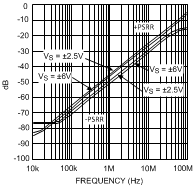
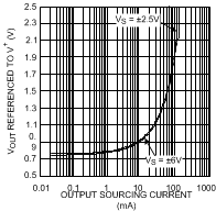
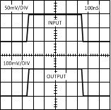
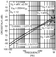
6.7 Typical Performance Characteristics
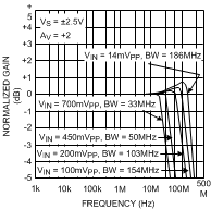
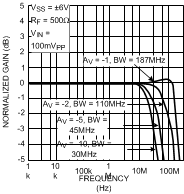
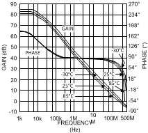
VS = ±2.5 V, RL = 100 Ω, AV = +2, RF = 500 Ω
VS = ±2.5 V, RL = 100 Ω, AV = +2, RF = 500 Ω
@ VS = ±2.5 V
@ VS = ±6 V
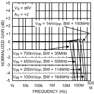
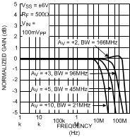
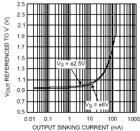
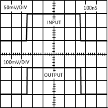
VS = ±6 V, RL = 100 Ω, AV = +2, RF = 500 Ω
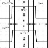
VS = ±6 V, RL = 100 Ω, AV = +2, RF = 500 Ω

@ VS = ±2.5 V