SNOS986E December 2001 – July 2014 LMH6622
PRODUCTION DATA.
- 1 Features
- 2 Applications
- 3 Description
- 4 Revision History
- 5 Pin Configuration and Functions
- 6 Specifications
- 7 Parameter Measurement Information
- 8 Detailed Description
- 9 Application and Implementation
- 10Power Supply Recommendations
- 11Layout
- 12Device and Documentation Support
- 13Mechanical, Packaging, and Orderable Information
封装选项
机械数据 (封装 | 引脚)
散热焊盘机械数据 (封装 | 引脚)
- DGK|8
订购信息
9 Application and Implementation
9.1 DSL Receive Channel Applications
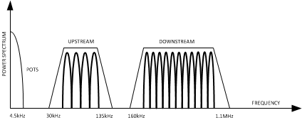 Figure 35. ADSL Signal Description
The LMH6622 is a dual, wideband operational amplifier designed for use as a DSL line receiver. In the receive band of a Customer Premises Equipment (CPE) ADSL modem it is possible that as many as 255 Discrete Multi-Tone (DMT) QAM signals will be present, each with its own carrier frequency, modulation, and signal level. The ADSL standard requires a line referred noise power density of -140 dBm/Hz within the CPE receive band of 100 KHz to 1.1 MHz. The CPE driver output signal will leak into the receive path because of full duplex operation and the imperfections of the hybrid coupler circuit. The DSL analog front end must incorporate a receiver pre-amp which is both low noise and highly linear for ADSL-standard operation. The LMH6622 is designed for the twin performance parameters of low noise and high linearity.
Applications ranging from +5 V to +12 V or ±2.5 V to ±6 V are fully supported by the LMH6622. In Figure 36, the LMH6622 is used as an inverting summing amplifier to provide both received pre-amp channel gain and driver output signal cancellation, that is, the function of a hybrid coupler.
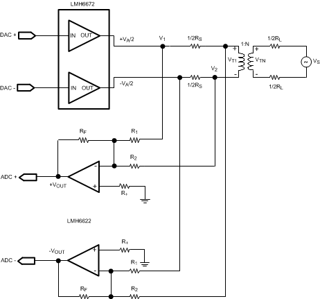 Figure 36. ADSL Receive Applications Circuit
The two RS resistors are used to provide impedance matching through the 1:N transformer.

where
- RL is the impedance of the twisted pair line
- N is the turns ratio of the transformer
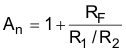
The resistors R2 and RF are used to set the receive gain of the pre-amp. The receive gain is selected to meet the ADC full-scale requirement of a DSL chipset.
Resistor R1 and R2 along with RF are used to achieve cancellation of the output driver signal at the output of the receiver.
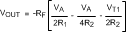
Since the LMH6622 is configured as an inverting summing amplifier, VOUT is found to be,

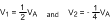
The expression for V1 and V2 can be found by using superposition principle.
When VS = 0,
When VA = 0,

Therefore,
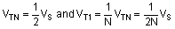
And then,
Setting R1 = 2*R2 to cancel unwanted driver signal in the receive path, then we have

We can also find that,
And then

In conclusion, the peak-to-peak voltage to the ADC would be,

9.2 Receive Channel Noise Calculation
The circuit of Figure 36 also has the characteristic that it cancels noise power from the drive channel.
The noise gain of the receive pre-amp is found to be:
Noise power at each of the output of LMH6622:

where
- Vn is the Input referred voltage noise
- in is the Input referred current noise
- inon-inv is the Input referred non-inverting current noise
- iinv is the Input referred inverting current noise
- k is the Boltzmann’s constant, K = 1.38 x 10⁻²³
- T is the Resistor temperature in k
- R+ is the source resistance at the non-inverting input to balance offset voltage, typically very small for this inverting summing applications
For a voltage feedback amplifier,

Therefore, total output noise from the differential pre-amp is:

The factor '2 ' appears here because of differential output.
9.3 Differential Analog-to-Digital Driver
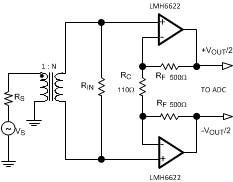 Figure 37. Circuit for Differential A/D Driver
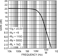
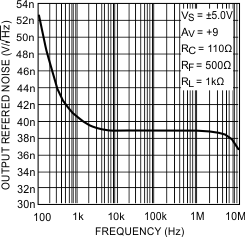
The LMH6622 is a low noise, low distortion high speed operational amplifier. The LMH6622 comes in either SOIC-8 or VSSOP-8 packages. Because two channels are available in each package the LMH6622 can be used as a high dynamic range differential amplifier for the purpose of driving a high speed analog-to-digital converter. Driving a 1 kΩ load, the differential amplifier of Figure 37 provides 20 dB gain, a flat frequency response up to 6 MHz, and harmonic distortion that is lower than 80 dBc. This circuit makes use of a transformer to convert a single-ended signal to a differential signal. The input resistor RIN is chosen by the following equation,

The gain of this differential amplifier can be adjusted by RC and RF,

See Figure 38 and Figure 39 below for plots related to the discussion of Figure 37.
9.4 Typical Application
See Figure 40 for application circuit.
Figure 40. ADSL Receive Applications Circuit
9.4.1 Design Requirements
All normal precautions / considerations with Op Amps apply
9.4.2 Detailed Design Procedure
- Use power supply decoupling capacitors close to supply pins
- Beware of junction temperature rise at elevated ambient temperature and / or heavy output(s) load current especially at higher supply voltages
- Ground plane near sensitive input pins can be removed to minimize parasitic capacitance