SNOS469J April 2000 – January 2015 LM8261
PRODUCTION DATA.
5 Pin Configuration and Functions
5-Pin SOT-23
Package DBV
(Top View)
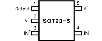
Pin Functions
| PIN | I/O | DESCRIPTION | |
|---|---|---|---|
| NUMBER | NAME | ||
| 1 | Output | O | Output |
| 2 | V- | I | Negative Supply |
| 3 | IN+ | I | Non-inverting input |
| 4 | IN- | I | Inverting Input |
| 5 | V+ | I | Positive Supply |