ZHCSDH1A October 2015 – May 2016 LM5175
PRODUCTION DATA.
- 1 特性
- 2 应用
- 3 说明
- 4 简化电路原理图
- 5 修订历史记录
- 6 Pin Configuration and Functions
- 7 Specifications
-
8 Detailed Description
- 8.1 Overview
- 8.2 Functional Block Diagram
- 8.3
Feature Description
- 8.3.1 Fixed Frequency Valley/Peak Current Mode Control with Slope Compensation
- 8.3.2 VCC Regulator and Optional BIAS Input
- 8.3.3 Enable/UVLO
- 8.3.4 Soft-Start
- 8.3.5 Overcurrent Protection
- 8.3.6 Average Input/Output Current Limiting
- 8.3.7 CCM/DCM Operation
- 8.3.8 Frequency and Synchronization (RT/SYNC)
- 8.3.9 Frequency Dithering
- 8.3.10 Output Overvoltage Protection (OVP)
- 8.3.11 Power Good (PGOOD)
- 8.3.12 Gm Error Amplifier
- 8.3.13 Integrated Gate Drivers
- 8.3.14 Thermal Shutdown
- 8.4 Device Functional Modes
-
9 Application and Implementation
- 9.1 Application Information
- 9.2
Typical Application
- 9.2.1 Design Requirements
- 9.2.2
Detailed Design Procedure
- 9.2.2.1 Frequency
- 9.2.2.2 VOUT
- 9.2.2.3 Inductor Selection
- 9.2.2.4 Output Capacitor
- 9.2.2.5 Input Capacitor
- 9.2.2.6 Sense Resistor (RSENSE)
- 9.2.2.7 Slope Compensation
- 9.2.2.8 UVLO
- 9.2.2.9 Soft-Start Capacitor
- 9.2.2.10 Dither Capacitor
- 9.2.2.11 MOSFETs QH1 and QL1
- 9.2.2.12 MOSFETs QH2 and QL2
- 9.2.2.13 Frequency Compensation
- 9.2.3 Application Curves
- 10Power Supply Recommendations
- 11Layout
- 12器件和文档支持
- 13机械、封装和可订购信息
封装选项
机械数据 (封装 | 引脚)
散热焊盘机械数据 (封装 | 引脚)
订购信息
7 Specifications
7.1 Absolute Maximum Ratings(1)
| MIN | MAX | UNIT | ||
|---|---|---|---|---|
| VIN, EN/UVLO, VISNS, VOSNS, ISNS(+), ISNS(–) | –0.3 | 60 | V | |
| BIAS | –0.3 | 40 | ||
| FB, SS, DITH, RT/SYNC, SLOPE, COMP | –0.3 | 3.6 | ||
| SW1, SW2 | –1 | 60 | ||
| SW1, SW2 (20 ns transient) | –3.0 | 65 | ||
| VCC, MODE, PGOOD | –0.3 | 8.5 | ||
| LDRV1, LDRV2 | –0.3 | 8.5 | ||
| BOOT1, HDRV1 with respect to SW1 | –0.3 | 8.5 | ||
| BOOT2, HDRV2 with respect to SW2 | –0.3 | 8.5 | ||
| BOOT1, BOOT2 | –0.3 | 68 | ||
| CS, CSG | –0.3 | 0.3 | ||
| Operating junction temperature | –40 | 150 | °C | |
| Storage temperature, Tstg | -65 | 150 | ||
(1) Stresses beyond those listed under Absolute Maximum Ratings may cause permanent damage to the device. These are stress ratings only, which do not imply functional operation of the device at these or any other conditions beyond those indicated under Recommended Operating Conditions. Exposure to absolute-maximum-rated conditions for extended periods may affect device reliability.
7.2 ESD Ratings
| VALUE | UNIT | ||
|---|---|---|---|
| VESD(1) | Human body model (HBM) ESD stress voltage(2) | ±2000 | V |
| Charged device model (CDM) ESD stress voltage(3) | ±750 |
(1) Electrostatic discharge (ESD) to measure device sensitivity and immunity to damage caused by assembly line electrostatic discharges into the device.
(2) Level listed above is the passing level per ANSI/ESDA/JEDEC JS-001. JEDEC document JEP155 states that 500 V HBM allows safe manufacturing with a standard ESD control process.
(3) Level listed above is the passing level per EIA-JEDEC JESD22-C101. JEDEC document JEP157 states that 250 V CDM allows safe manufacturing with a standard ESD control process.
7.3 Recommended Operating Conditions
over operating free-air temperature range (unless otherwise noted)(1)| MIN | NOM | MAX | UNIT | ||
|---|---|---|---|---|---|
| VIN | Input voltage range | 3.5 | 42 | V | |
| BIAS | Bias supply voltage range | 8 | 36 | ||
| VOUT | Output voltage range | 0.8 | 55 | ||
| EN/UVLO | Enable voltage range | 0 | 42 | ||
| ISNS(+), ISNS(-) | Average current sense common mode range | 0 | 55 | ||
| TJ | Operating temperature range(2) | –40 | 125 | °C | |
| Fsw | Operating frequency range | 100 | 600 | kHz | |
(1) Recommended Operating Conditions are conditions under the device is intended to be functional. For specifications and test conditions, see Electrical Characteristics .
(2) High junction temperatures degrade operating lifetimes. Operating lifetime is de-rated for junction temperatures greater than 125°C.
7.4 Thermal Information
| THERMAL METRIC(1) | LM5175 | UNIT | ||
|---|---|---|---|---|
| HTSSOP | QFN | |||
| 28 PINS | 28 PINS | |||
| RθJA | Junction-to-ambient thermal resistance | 33.1 | 34.7 | °C/W |
| RθJC(top) | Junction-to-case (top) thermal resistance | 17.7 | 26.6 | |
| RθJB | Junction-to-board thermal resistance | 14.9 | 6.3 | |
| ψJT | Junction-to-top characterization parameter | 0.4 | 0.3 | |
| ψJB | Junction-to-board characterization parameter | 14.7 | 6.2 | |
| RθJC(bot) | Junction-to-case (bottom) thermal resistance | 1.1 | 2.0 | |
(1) For more information about traditional and new thermal metrics, see the IC Package Thermal Metrics application report, SPRA953.
7.5 Electrical Characteristics
Typical values correspond to TJ = 25°C. Minimum and maximum limits apply over the –40°C to 125°C junction temperature range unless otherwise stated. VIN = 24 V unless otherwise stated.(1)| PARAMETER | TEST CONDITION | MIN | TYP | MAX | UNIT | ||
|---|---|---|---|---|---|---|---|
| SUPPLY VOLTAGE (VIN) | |||||||
| VIN | Operating input voltage | 3.5 | 42 | V | |||
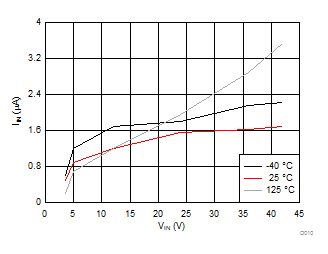
| IQ | VIN shutdown current | VEN/UVLO = 0 V | 1.4 | 10 | µA | ||
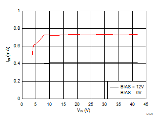
| VIN standby current | VEN/UVLO = 1.1 V, non-switching | 0.7 | 2 | ||||
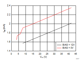
| VIN operating current | VEN/UVLO = 2 V, VFB = 0.9 V | 1.65 | 4 | mA | |||
| VCC | |||||||
| VVCC(VIN) | Regulation voltage | VBIAS = 0 V, VCC open | 6.95 | 7.35 | 7.88 | V | |
| VUV(VCC) | VCC Undervoltage lockout | VCC increasing | 3.11 | 3.27 | 3.43 | ||
| Undervoltage hysteresis | 160 | mV | |||||
| IVCC | VCC current limit | VVCC = 0 V | 65 | mA | |||
| ROUT(VCC) | VCC regulator output impedance | IVCC = 30 mA, VIN = 3.5 V | 9.3 | 16 | Ω | ||
| BIAS | |||||||
| VBIAS(SW) | BIAS switchover voltage | VIN = 24 V | 7.25 | 8 | 8.75 | V | |
| EN/UVLO | |||||||
| VEN(STBY) | Standby threshold | EN/UVLO rising | 0.55 | 0.79 | 0.97 | V | |
| IEN(STBY) | Standby source current | VEN/UVLO = 1.1 V | 1 | 2 | 3 | µA | |
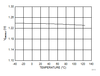
| VEN(OP) | Operating threshold | EN/UVLO rising | 1.17 | 1.23 | 1.29 | V | |
| ΔIHYS(OP) | Operating hysteresis current | VEN/UVLO = 2.4 V | 1.5 | 3.5 | 5.5 | µA | |
| SS | |||||||
| ISS | Soft-start pull up current | VSS = 0 V | 4.30 | 5.65 | 7.25 | µA | |
| VSS(CL) | SS clamp voltage | SS open | 1.27 | V | |||
| VFB - VSS | FB to SS offset | VSS = 0 V | -15 | mV | |||
| EA (ERROR AMPLIFIER) | |||||||
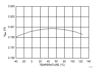
| VREF | Feedback reference voltage | FB = COMP | 0.788 | 0.800 | 0.812 | V | |
| gmEA | Error amplifier gm | 1.27 | mS | ||||
| ISINK/ISOURCE | COMP sink/source current | VFB=VREF ± 300 mV | 280 | µA | |||
| ROUT | Amplifier output resistance | 20 | MΩ | ||||
| BW | Unity gain bandwidth | 2 | MHz | ||||
| IBIAS(FB) | Feedback pin input bias current | FB in regulation | 100 | nA | |||
| FREQUENCY | |||||||
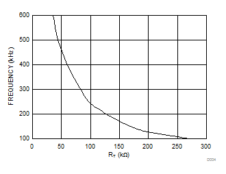
| fSW(1) | Switching Frequency 1 | RT = 133 kΩ | 180 | 200 | 220 | kHz | |
| fSW(2) | Switching Frequency 2 | RT = 47 kΩ | 430 | 500 | 565 | ||
| DITHER | |||||||
| IDITHER | Dither source/sink current | 10.5 | µA | ||||
| VDITHER | Dither high threshold | 1.27 | V | ||||
| Dither low threshold | 1.16 | ||||||
| SYNC | |||||||
| VSYNC | Sync input high threshold | 2.1 | V | ||||
| Sync input low threshold | 1.2 | ||||||
| PWSYNC | Sync input pulse width | 75 | 500 | ns | |||
| CURRENT LIMIT | |||||||
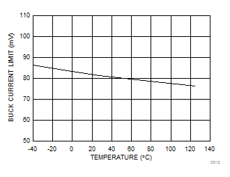
| VCS(BUCK) | Buck current limit threshold (Valley) | VIN = VVISNS = 24 V, VVOSNS = 12 V, VSLOPE = 0 V, TJ = 25°C | 53.2 | 76 | 98 | mV | |
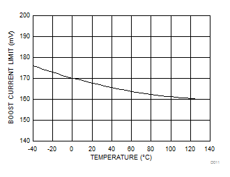
| VCS(BOOST) | Boost current limit threshold (Peak) | VIN = VVISNS = 12 V, VVOSNS = 18 V, VSLOPE = 0 V, TJ = 25°C | 119 | 170 | 221 | ||
| IBIAS(CS/CSG) | CS/CSG pin bias current | VCS = VCSG = 0 V | -75 | µA | |||
| IOFFSET(CS/CSG) | CSG pin bias current | VCS = VCSG = 0 V | 14 | ||||
| CONSTANT CURRENT LOOP | |||||||
| VSNS | Average current loop regulation target | VISNS(-) = 24 V, sweep ISNS(+), VSS = 0.8 V | 43 | 50 | 57 | mV | |
| ISNS | ISNS(+)/ISNS(–) pin bias currents | VISNS(+) = VISNS(–) = VIN = 24 V | 7 | µA | |||
| Gm | gm of soft-start pull down amplifier | VISNS(+)–VISNS(–) = 55 mV, VSS = 0.5 V | 1 | mS | |||
| SLOPE | |||||||
| ISLOPE | Buck adaptive slope current | VIN = VVINSNS = 24 V, VVOSNS = 12 V, VSLOPE = 0 V | 24 | 30 | 35 | µA | |
| Boost adaptive slope current | VIN = VVINSNS = 12 V, VVOSNS = 18 V, VSLOPE = 0 V | 13 | 17 | 21 | |||
| gmSLOPE | Slope compensation amplifier gm | 2 | µS | ||||
| MODE | |||||||
| IMODE | Source current out of MODE pin | 17 | 20 | 23 | µA | ||
| VDCM_HIC | DCM with hiccup threshold | 0.60 | 0.7 | 0.76 | V | ||
| VCCM_HIC | CCM with hiccup threshold | 1.18 | 1.28 | 1.38 | |||
| VCCM | CCM no hiccup threshold | 2.22 | 2.4 | 2.6 | |||
| PGOOD | |||||||
| VPGD | PGOOD trip threshold for falling FB | Measured with respect to VREF | –9 | % | |||
| PGOOD trip threshold for rising FB | Measured with respect to VREF | 10 | % | ||||
| Hysteresis | 1.6 | % | |||||
| ILEAK(PGD) | PGOOD leakage current | 100 | nA | ||||
| ISINK(PGD) | PGOOD sink current | VPGOOD = 0.4 V | 2 | 4.2 | 6.5 | mA | |
| OUTPUT OVP | |||||||
| VOVP | Output overvoltage threshold | At the FB pin | 0.86 | V | |||
| Hysteresis | 21 | mV | |||||
| NMOS DRIVERS | |||||||
| IHDRV1,2 | Driver peak source current | VBOOT - VSW = 7 V | 1.8 | A | |||
| Driver peak sink current | VBOOT - VSW = 7 V | 2.2 | |||||
| ILDRV1,2 | Driver peak source current | 1.8 | |||||
| Driver peak sink current | 2.2 | ||||||
| RHDRV1,2 | Driver pull up resistance | VBOOT - VSW = 7 V | 1.9 | Ω | |||
| Driver pull down resistance | VBOOT - VSW = 7 V | 1.3 | |||||
| VUV(BOOT1,2) | BOOT1,2 to SW1,2 UVLO threshold | HDRV1,2 shut off | 2.73 | V | |||
| BOOT1,2 to SW1,2 UVLO hysteresis | HDRV1,2 start switching | 280 | mV | ||||
| BOOT1,2 to SW1,2 threshold for refresh pulse | 4.45 | V | |||||
| RLDRV1,2 | Driver pull up resistance | IDRV1,2 = 0.1 A | 2 | Ω | |||
| Driver pull down resistance | IDRV1,2 = 0.1 A | 1.5 | |||||
| tDT1 | Dead time HDRV1,2 off to LDRV1,2 on | 55 | ns | ||||
| tDT2 | Dead time LDRV1,2 off to HDRV1,2 on | 55 | |||||
| THERMAL SHUTDOWN | |||||||
| TSD | Thermal shutdown temperature | 165 | °C | ||||
| TSD(HYS) | Thermal shutdown hysteresis | 15 | |||||
(1) All minimum and maximum limits are specified by correlating the electrical characteristics to process and temperature variations and applying statistical process control.
7.6 Typical Characteristics
At TA = 25°C, unless otherwise stated.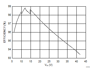
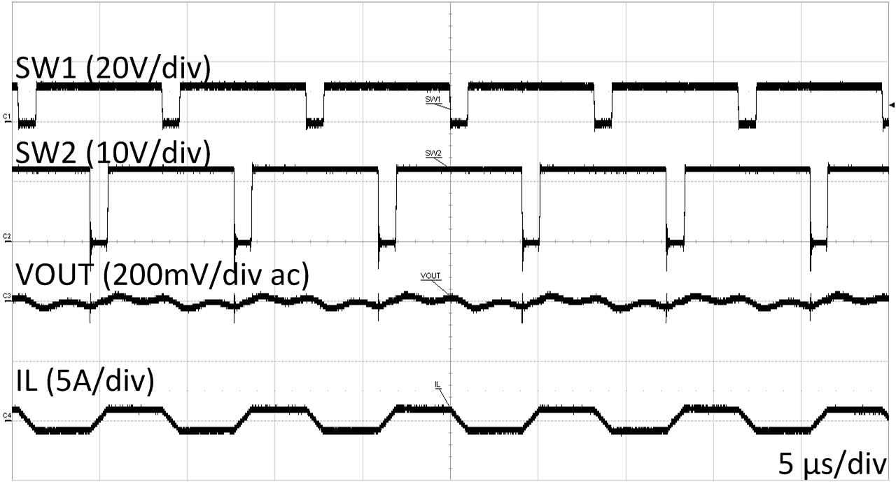
| VOUT=12 V | Fsw=300 kHz | L1=4.7 μH |
| IOUT=3 A |
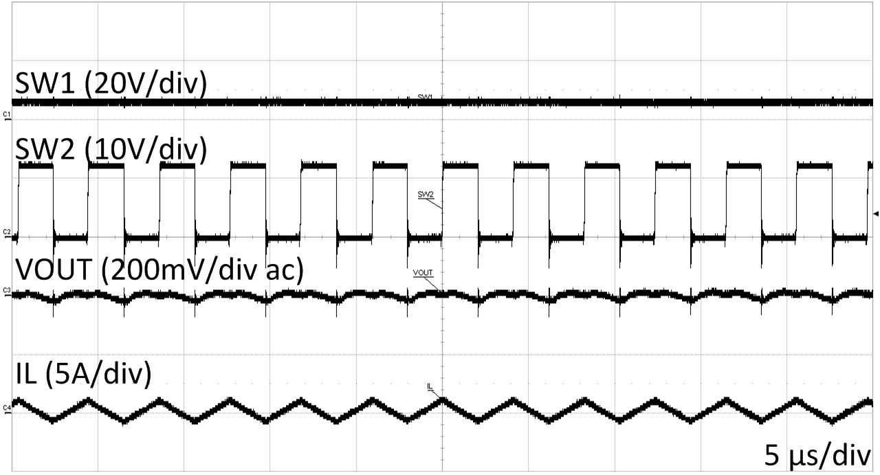
| VOUT=12 V | VIN=6 V | |
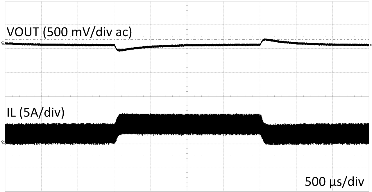
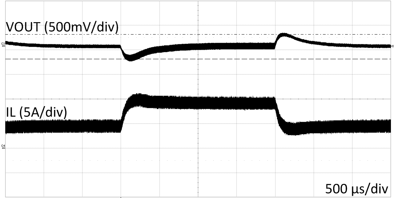
| VIN=24 V | VOUT=12 V | Load 2A to 4A |
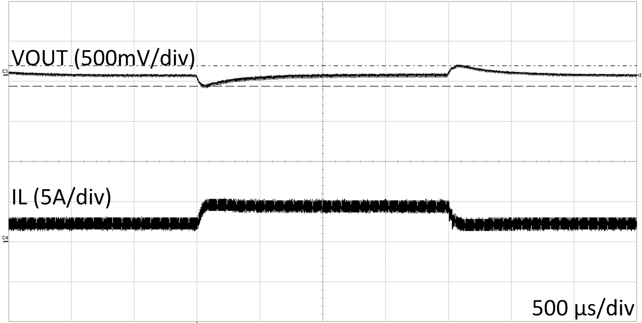
| VIN=12 V | VOUT=12 V | Load 2A to 4A |
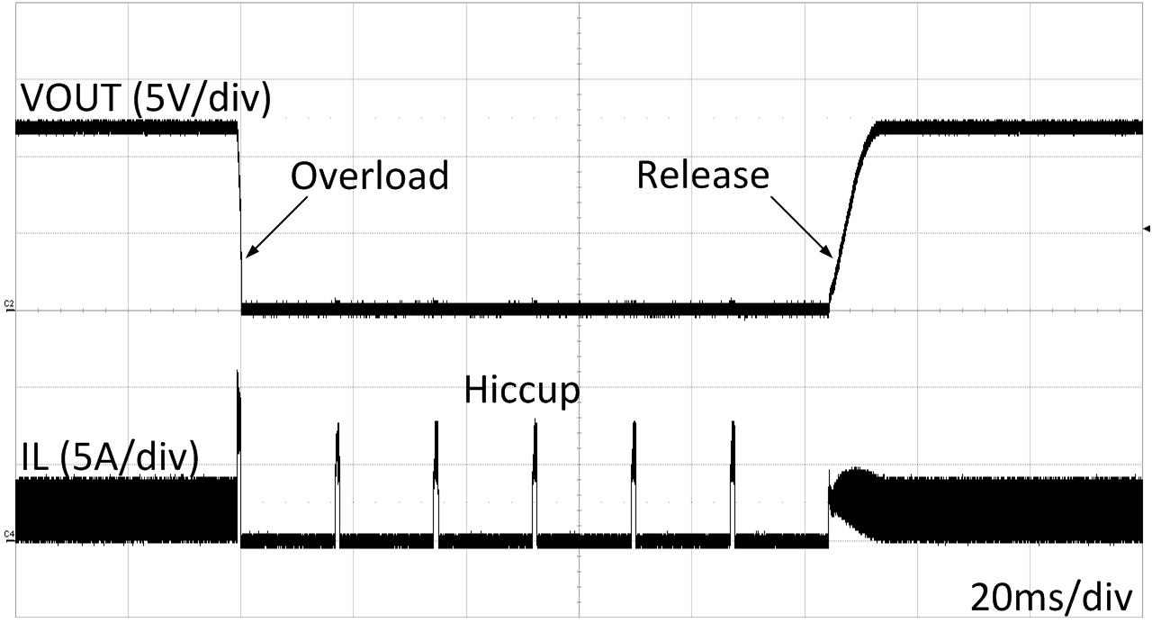
| VIN=24 V | VOUT=12 V | Hiccup Enabled |
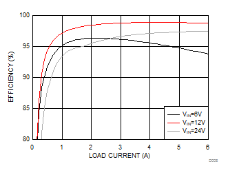
| VOUT =12 V | Fsw=300 kHz | L1=4.7 μH |
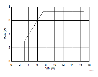
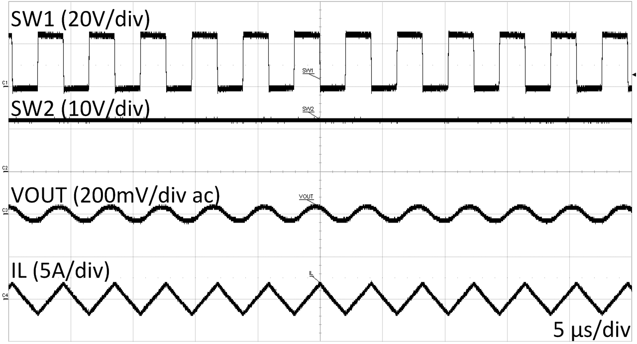
| VOUT=12 V | VIN=24 V | |
| VOUT=12 V | VIN=12 V | |
| VIN=6 V | VOUT=12 V | Load 2A to 4A |
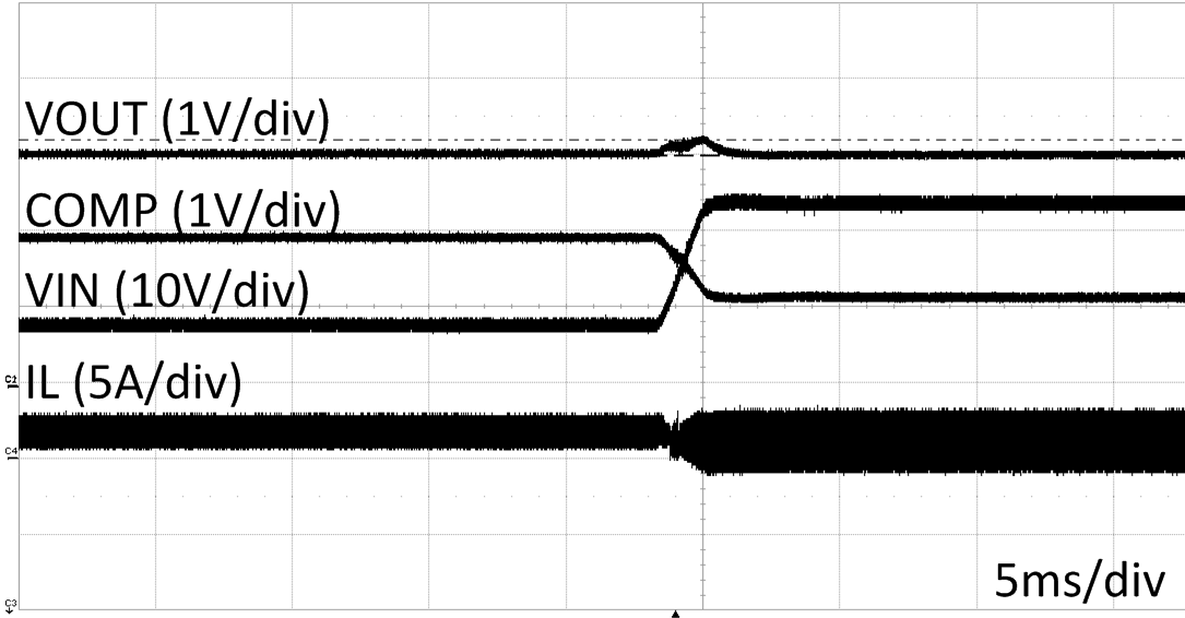
| VIN=8 V to 24 V | VOUT=12 V | IOUT=1A |