SNVS628H October 2009 – December 2019 LM5060
PRODUCTION DATA.
- 1 Features
- 2 Applications
- 3 Description
- 4 Revision History
- 5 Pin Configuration and Functions
- 6 Specifications
- 7 Detailed Description
-
8 Application and Implementation
- 8.1 Application Information
- 8.2
Typical Applications
- 8.2.1
Example Number 1: LM5060EVAL Design
- 8.2.1.1 Design Requirements
- 8.2.1.2
Detailed Design Procedure
- 8.2.1.2.1 VDS Fault Detection and Selecting Sense Pin Resistor RS
- 8.2.1.2.2 Turn-On Time
- 8.2.1.2.3 Fault Detection Delay Time
- 8.2.1.2.4 MOSFET Selection
- 8.2.1.2.5 Input and Output Capacitors
- 8.2.1.2.6 UVLO, OVP
- 8.2.1.2.7 POWER GOOD Indicator
- 8.2.1.2.8 Input Bypass Capacitor
- 8.2.1.2.9 Large Load Capacitance
- 8.2.1.3 Application Curves
- 8.2.2 Example Number 2: Reverse Polarity Protection With Diodes
- 8.2.3 Example Number 3: Reverse Polarity Protection With Resistor
- 8.2.1
Example Number 1: LM5060EVAL Design
- 9 Power Supply Recommendations
- 10Layout
- 11Device and Documentation Support
- 12Mechanical, Packaging, and Orderable Information
8.2.1.2.9 Large Load Capacitance
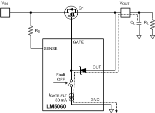
Figure 32 shows an application with a large load capacitance CL. Assume a worst case turn off scenario where Vin remains at the same voltage as CL and RL is a high impedance. The body diode of Q1 will not conduct any current and all the charge on CL is dissipated through the LM5060 internal circuitry. The dotted line in Figure 32 shows the path of this current flow. Initially the power dissipated by the LM5060 is calculated with the formula:
where
- IGATE-FLT is the sink current of the LM5060 gate control
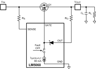
In applications with a high input voltage and very large output capacitance, the discharge current can be limited by an additional discharge resistor RO in series with the OUT pin as shown in Figure 33. This resistor will influence the current limit threshold, so the value of RS will need to be readjusted.
 Figure 32. Discharge Path of Possible Load Capacitor
 In applications exposed to reverse polarity on the input and a large load capacitance on the output, a current limiting resistor in series with the OUT pin is required to protect the LM5060 OUT pin from reverse currents exceeding 25 mA. Figure 33 shows the resistor RO in the trace to the OUT pin.
 Figure 33. Current Limiting Resistor RO for Special Cases
 If a RO resistor in the OUT path is used, the current sensing will become less accurate since RO has some variability as well as the current into the OUT pin. The OUT pin current is specified in the Electrical Characteristics section as IOUT-EN. A RO resistor design compromise for protection of the OUT pin and a maintaining VDS sensing accuracy can be achieved. See the Reverse Polarity Protection With a Resistor section for more details on how to calculate a reasonable RO value.