SNVS628H October   2009  – December 2019 LM5060

PRODUCTION DATA.  

  1. Features
  2. Applications
  3. Description
    1.     Device Images
      1.      Typical Application Circuit
  4. Revision History
  5. Pin Configuration and Functions
    1.     Pin Functions
  6. Specifications
    1. 6.1 Absolute Maximum Ratings
    2. 6.2 ESD Ratings
    3. 6.3 Recommended Operating Conditions
    4. 6.4 Thermal Information
    5. 6.5 Electrical Characteristics
    6. 6.6 Typical Characteristics
  7. Detailed Description
    1. 7.1 Overview
    2. 7.2 Functional Block Diagram
    3. 7.3 Feature Description
    4. 7.4 Device Functional Modes
      1. 7.4.1 Power-Up Sequence
      2. 7.4.2 Status Conditions
  8. Application and Implementation
    1. 8.1 Application Information
      1. 8.1.1  Gate Control
      2. 8.1.2  Fault Timer
      3. 8.1.3  VGS Considerations
      4. 8.1.4  VDS Fault Condition
      5. 8.1.5  Overcurrent Fault
      6. 8.1.6  Restart After Overcurrent Fault Event
      7. 8.1.7  Enable
      8. 8.1.8  UVLO
      9. 8.1.9  OVP
      10. 8.1.10 Restart After OVP Event
      11. 8.1.11 nPGD Pin
    2. 8.2 Typical Applications
      1. 8.2.1 Example Number 1: LM5060EVAL Design
        1. 8.2.1.1 Design Requirements
        2. 8.2.1.2 Detailed Design Procedure
          1. 8.2.1.2.1 VDS Fault Detection and Selecting Sense Pin Resistor RS
          2. 8.2.1.2.2 Turn-On Time
          3. 8.2.1.2.3 Fault Detection Delay Time
          4. 8.2.1.2.4 MOSFET Selection
          5. 8.2.1.2.5 Input and Output Capacitors
          6. 8.2.1.2.6 UVLO, OVP
          7. 8.2.1.2.7 POWER GOOD Indicator
          8. 8.2.1.2.8 Input Bypass Capacitor
          9. 8.2.1.2.9 Large Load Capacitance
        3. 8.2.1.3 Application Curves
      2. 8.2.2 Example Number 2: Reverse Polarity Protection With Diodes
        1. 8.2.2.1 Design Requirements
        2. 8.2.2.2 Application Curve
      3. 8.2.3 Example Number 3: Reverse Polarity Protection With Resistor
        1. 8.2.3.1 Design Requirements
        2. 8.2.3.2 Detailed Design Procedure
          1. 8.2.3.2.1 Reverse Polarity Protection With a Resistor
          2. 8.2.3.2.2 Fault Detection With RS and RO
        3. 8.2.3.3 Application Curves
  9. Power Supply Recommendations
  10. 10Layout
    1. 10.1 Layout Guidelines
    2. 10.2 Layout Example
    3. 10.3 Thermal Considerations
  11. 11Device and Documentation Support
    1. 11.1 Documentation Support
      1. 11.1.1 Related Documentation
    2. 11.2 Community Resources
    3. 11.3 Trademarks
    4. 11.4 Electrostatic Discharge Caution
    5. 11.5 Glossary
  12. 12Mechanical, Packaging, and Orderable Information

封装选项

机械数据 (封装 | 引脚)
散热焊盘机械数据 (封装 | 引脚)
订购信息

Application Curves

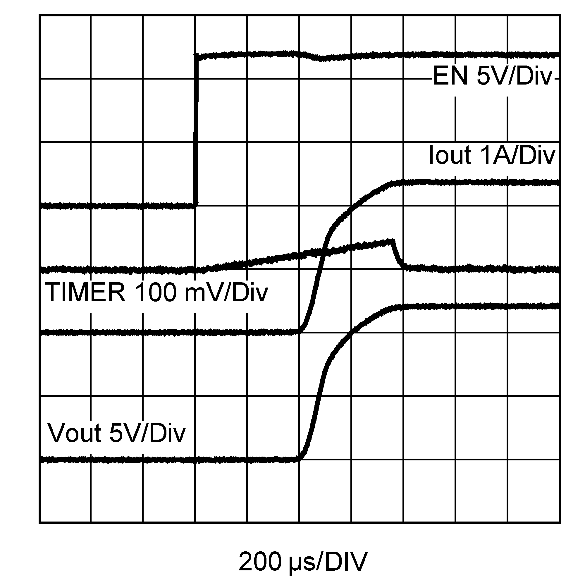
LM5060 wvfm01_startup1_snvs628.pngFigure 34. Start-Up Waveform
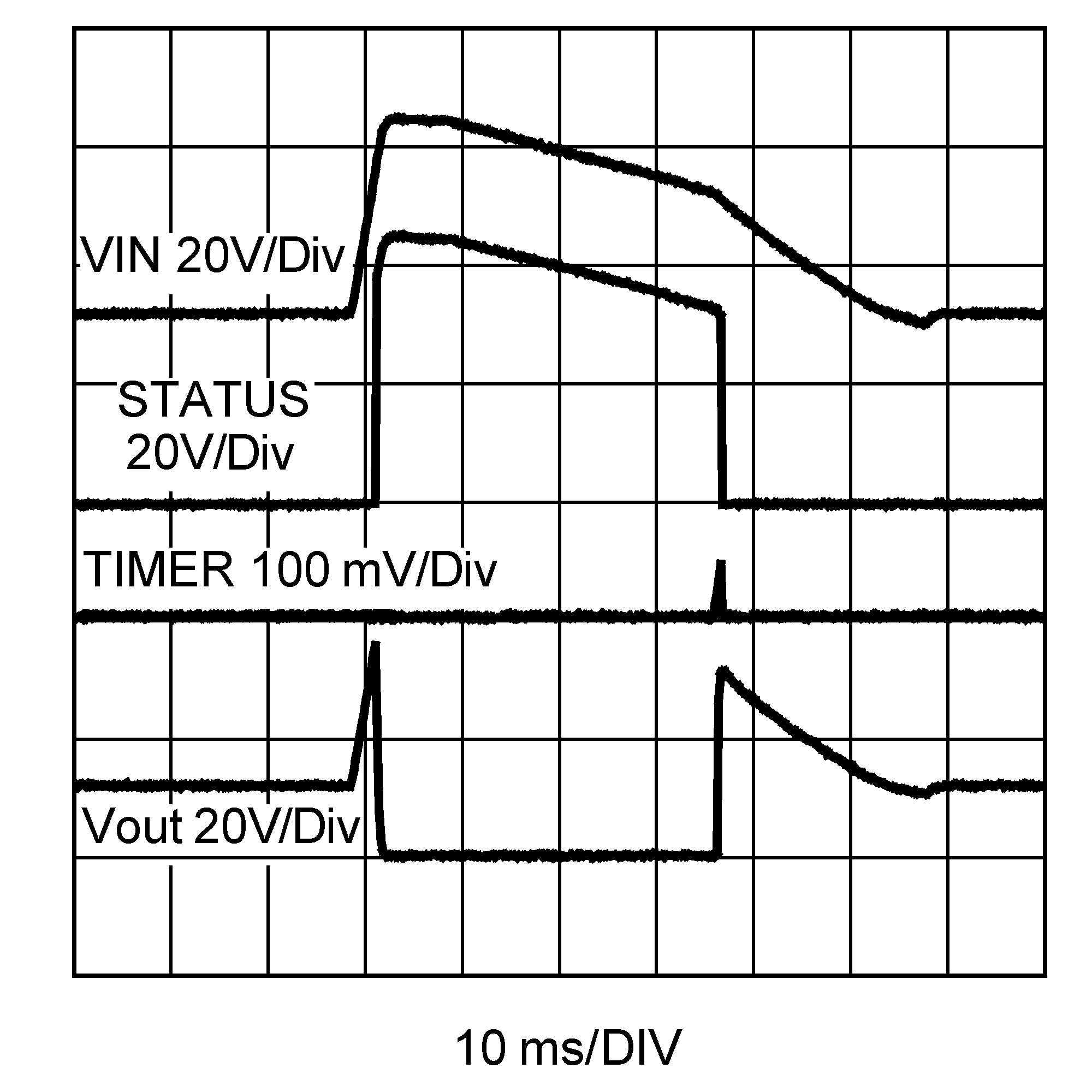
LM5060 wvfm03_ovp_behavior_snvs628.pngFigure 36. OVP Behavior
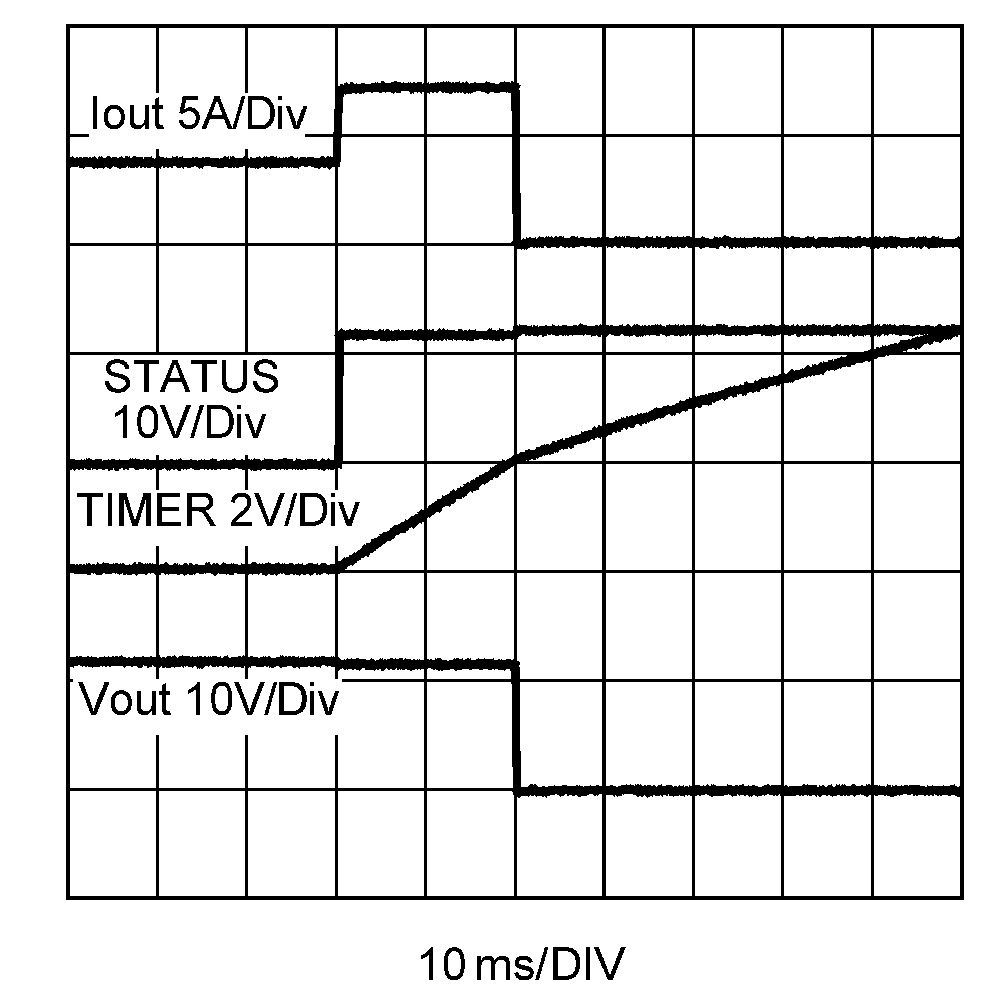
LM5060 wvfm05_fault_behavior_snvs628.pngFigure 38. Fault Behavior
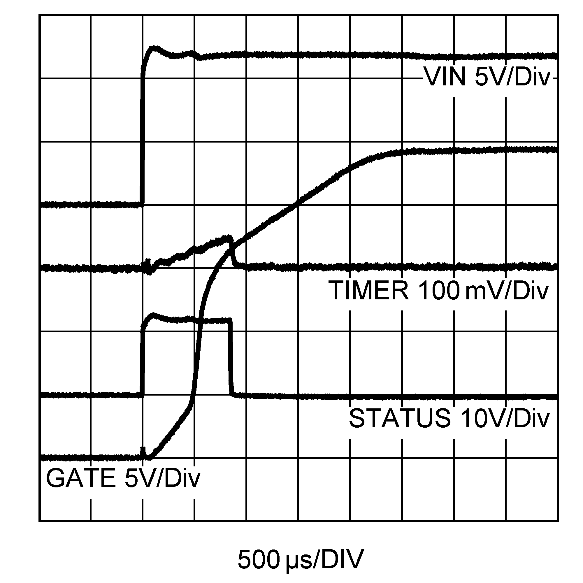
LM5060 wvfm02_startup2_snvs628.pngFigure 35. Start-Up Waveform
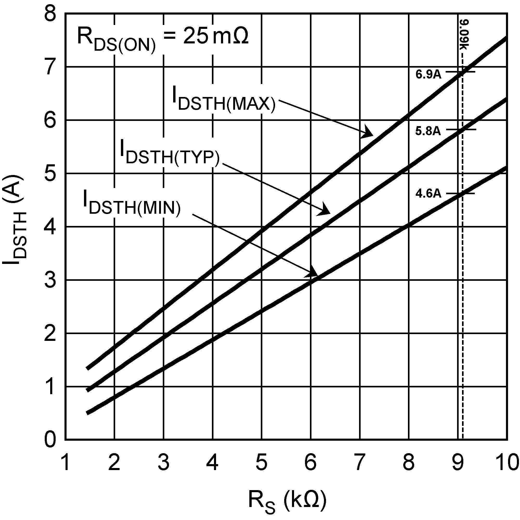
LM5060 wvfm04_rs_vs_idsth_snvs628.pngFigure 37. RS vs IDSTH for RDS(ON) = 25 mΩ