SNVS293F December 2004 – August 2016 LM5025A
PRODUCTION DATA.
- 1 Features
- 2 Applications
- 3 Description
- 4 Revision History
- 5 Pin Configuration and Functions
- 6 Specifications
- 7 Detailed Description
- 8 Application and Implementation
- 9 Power Supply Recommendations
- 10Layout
- 11Device and Documentation Support
- 12Mechanical, Packaging, and Orderable Information
10 Layout
10.1 Layout Guidelines
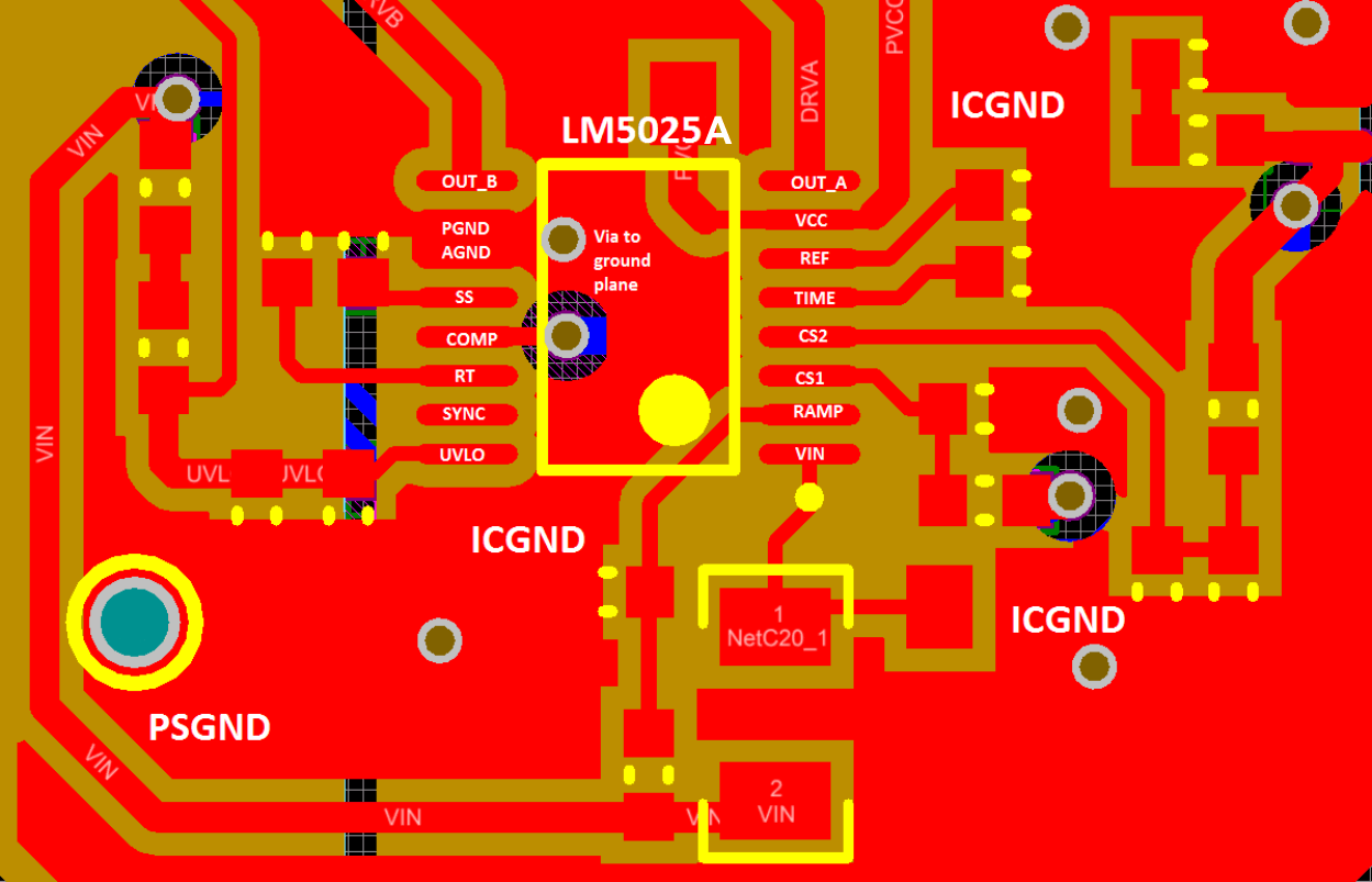
- Connect two grounds PGND (power ground) and AGND (analog ground) directly as device ground ICGND. The connection must be as close to the pins as possible.
- If there are multiple PCB layers and there is a inner ground layer, use two vias or one big via on GND and connect them to the inner ground layer (ICGND).
- The power stage ground PSGND must be separated with the ICGND. PSGND and ICGND must be connected at a single point close to the device.
- The bypass capacitors to the VCC pin and REF pin must be as close as possible to the pins and ground (ICGND).
- The filtering capacitors connected to CS1 and CS2 pins must have connections as short as possible to ICGND; if an inner ground layer is available, use vias to connect the capacitors to the ground layer (ICGND).
- The resistors and capacitors connected to the timing configuration pins must be as close as possible to the pins and ground (ICGND).
10.2 Layout Example
 Figure 23. LM5025A Layout Recommendation
10.3 Thermal Protection
Internal thermal shutdown circuitry is provided to protect the integrated circuit in the event the maximum junction temperature is exceeded. When activated, typically at 165°C, the controller is forced into a low-power standby state with the output drivers and the bias regulator disabled. The device restarts after the thermal hysteresis (typically 25°C). During a restart after thermal shutdown, the soft-start capacitor is fully discharged and then charged in the low current mode (1 µA) similar to a second level current limit event. The thermal protection feature is provided to prevent catastrophic failures from accidental device overheating.