ZHCSDU4E May 2005 – December 2014 LM5021
PRODUCTION DATA.
- 1 特性
- 2 应用
- 3 说明
- 4 修订历史记录
- 5 Pin Configuration and Functions
- 6 Specifications
- 7 Detailed Description
- 8 Application and Implementation
- 9 Power Supply Recommendations
- 10Layout
- 11器件和文档支持
- 12机械、封装和可订购信息
封装选项
机械数据 (封装 | 引脚)
散热焊盘机械数据 (封装 | 引脚)
- DGK|8
订购信息
7 Detailed Description
7.1 Overview
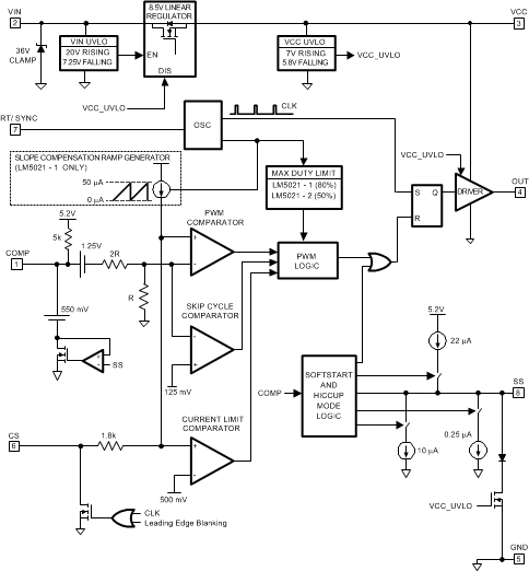
The LM5021 is a single ended current mode controller primarily intended for use in offline forward or flyback converters. It is also useful for boost converters. Low startup current and a wide UVLO hysteresis make low dissipation startup circuits simple to implement. An on board 7-V regulator supplies stable power for device operation and can supply external circuitry. A soft start function minimizes stresses during startup and allows the converter to come to steady state operating conditions gradually.
The device comes in two versions with different maximum duty cycles. The LM5021-1 has a maximum duty cycle of 80% while the LM5021-2 has a maximum duty cycle of 50%. For current mode control applications where the duty cycle can exceed 50%, slope compensation is implemented by simply adding a resistor between the LM5021-1 CS pin and the current sense filter capacitor.
Cycle-by-cycle overcurrent sensing provides robust protection. A 500-mV maximum current sense threshold minimizes power dissipation in supplies that sense the main switch current directly with a resistor. For a sustained overcurrent condition, the controller will enter a hiccup mode to reduce component stresses. The controller automatically restarts when the overload condition is removed.
The switching frequency is programmable using a single resistor connected from the RT pin to GND. For applications that require it, the switching frequency can be synchronized to an external clock source by capacitively coupling a pulse train into the RT pin.
Skip cycle operation is implemented to reduce input power and increase efficiency at light load conditions. For applications where this is not desirable, skip cycle operation may be disabled by adding an offset voltage to the CS pin.
7.2 Functional Block Diagram
7.3 Feature Description
7.3.1 PWM Comparator and Slope Compensation
The PWM comparator compares the current sense signal with the loop error voltage from the COMP pin. The COMP pin voltage is reduced by 1.25 V then attenuated by a 3:1 resistor divider. The PWM comparator input offset voltage is designed such that less than 1.25 V at the COMP pin will result in a zero duty cycle at the controller output.
For duty cycles greater than 50 percent, current mode control circuits are subject to sub-harmonic oscillation. By adding an additional fixed slope voltage ramp signal (slope compensation) to the current sense signal, this oscillation can be avoided. The LM5021-1 integrates this slope compensation by summing a ramp signal generated by the oscillator with the current sense signal. The slope compensation is generated by a current ramp driven through an internal 1.8 kΩ resistor connected to the CS pin. Additional slope compensation may be added by increasing the resistance between the current sense filter capacitor and the CS pin, thereby increasing the voltage ramp created by the oscillator current ramp. Since the LM5021-2 is not capable of duty cycles greater than 50%, there is no slope compensation feature in this device.
7.3.2 Current Limit and Current Sense
The LM5021 provides a cycle-by-cycle over current protection feature. Current limit is triggered by an internal current sense comparator threshold which is set at 500 mV. If the CS pin voltage plus the slope compensation voltage exceeds 500 mV, the OUT pin output pulse will be immediately terminated.
An RC filter, located near the LM5021, is recommended for the CS pin to attenuate the noise coupled from the power FET's gate to source. The CS pin capacitance is discharged at the end of each PWM clock cycle by an internal switch. The discharge switch remains on for an additional 90ns leading edge blanking interval to attenuate the current sense transient that occurs when the external power FET is turned on. In addition to providing leading edge blanking, this circuit also improves dynamic performance by discharging the current sense filter capacitor at the conclusion of every cycle.
The LM5021 CS comparator is very fast, and may respond to short duration noise pulses. Layout considerations are critical for the current sense filter and sense resistor. The capacitor associated with the CS filter must be placed very close to the device and connected directly to the pins of the IC (CS and GND). If a current sense transformer is used, both leads of the transformer secondary should be routed to the sense resistor, which should also be located close to the IC. If a current sense resistor located in the power FET's source is used for current sense, a low inductance resistor is required. In this case, all of the noise sensitive low current grounds should be connected in common near the IC and then a single connection should be made to the power ground (sense resistor ground point).
7.3.3 Oscillator, Shutdown and Sync Capability
A single external resistor connected between RT and GND pins sets the LM5021 oscillator frequency. The LM5021-2 device, with 50% maximum duty cycle, includes an internal flip-flop that divides the oscillator frequency by two. This method produces a precise 50% maximum duty cycle limit. Because of this frequency divider, the oscillator frequency of the LM5021-2 is actually twice the frequency of the gate drive output (OUT). For the LM5021-1 device, the oscillator frequency and the operational output frequency are the same. To set a desired output switching frequency (Fsw), the RT resistor can be calculated from:
LM5021-1:

LM5021-2:

The LM5021 can also be synchronized to an external clock. The external clock must have a higher frequency than the free running oscillator frequency set by the RT resistor. The clock signal should be capacitively coupled into the RT pin with a 100pF capacitor. A peak voltage level greater than 3.8 V at the RT pin is required for detection of the sync pulse. The dc voltage across the RT resistor is internally regulated at 2 V. Therefore, the ac pulse superimposed on the RT resistor must have 1.8-V or greater amplitude to successfully synchronize the oscillator. The sync pulse width should be set between 15 ns to 150 ns by the external components. The RT resistor is always required, whether the oscillator is free-running or externally synchronized. The RT resistor should be located very close to the device and connected directly to the pins of the LM5021 (RT and GND).
7.3.4 Gate Driver and Max Duty Cycle Limit
The LM5021 provides a gate driver (OUT), which can source peak current of 0.3A and sink 0.7A. The LM5021 is available in two duty-cycle limit options. The maximum output duty-cycle is typically 80% for the LM5021-1 option, and precisely equal to 50% for the LM5021-2 option. The maximum duty cycle function for the LM5021-2 is accomplished with an internal toggle flip-flop to ensure an accurate duty cycle limit. The internal oscillator frequency of the LM5021-2 is therefore twice the switching frequency of the PWM controller (OUT pin).
The 80% maximum duty-cycle function for the LM5021-1 is determined by the internal oscillator. For the LM5021-1 the internal oscillator frequency and the switching frequency of the PWM controller are the same.
7.3.5 Soft-Start
The soft-start feature allows the power converter to gradually reach the initial steady state operating point, thus reducing start-up stresses and current surges. An internal 22 µA current source charges an external capacitor connected to the SS pin. The capacitor voltage will ramp up slowly, limiting the COMP pin voltage and the duty cycle of the output pulses. The soft-start capacitor is also used to generate the hiccup mode delay time when the output of the switching power supply is continuously overloaded.
7.3.6 Hiccup Mode Overload Current Limiting
Hiccup mode is a method of protecting the power supply from over-heating and damage during an extended overload condition. When the output fault is removed the power supply will automatically restart.
Figure 8, Figure 9, and Figure 10 illustrate the equivalent circuit of the hiccup mode for LM5021 and the relevant waveforms. During start-up and in normal operation, the external soft-start capacitor Css is pulled up by a current source that delivers 22 µA to the SS pin capacitor. In normal operation, the soft-start capacitor continues to charge and eventually reaches the saturation voltage of the current source (VSS_OCV, nominally 5.2 V). During start-up the COMP pin voltage follows the SS capacitor voltage and gradually increases the peak current delivered by the power supply. When the output of the switching power supply reaches the desired voltage, the voltage feedback amplifier takes control of the COMP signal (via the opto-coupler). In normal operation the COMP level is held at an intermediate voltage between 1.25 V and 2.75 V controlled by the voltage regulation loop. When the COMP pin voltage is below 1.25 V, the duty-cycle is zero. When the COMP level is above 2.75 V, the duty cycle will be limited by the 0.5-V threshold of cycle-by-cycle current limit comparator.
If the output of the power supply is overloaded, the voltage regulation loop demands more current by increasing the COMP pin control voltage. When the COMP pin exceeds the over voltage detection threshold (VOVLD, nominally 4.6 V), the SS capacitor Css will be discharged by a 10 µA overload detection timer current source, IOVCS. If COMP remains above VOVLD long enough for the SS capacitor to discharge to the Hiccup mode threshold (VHIC, nominally 4.6 V), the controller enters the hiccup mode. The OUT pin is then latched low and the SS capacitor discharge current source is reduced from 10 µA to 0.25 µA, the dead-time current source, IDTCS. The SS pin voltage is slowly reduced until it reaches the Restart threshold (VRST, nominally 0.3 V). Then a new start-up sequence commences with 22 µA current source charging the capacitor CSS. The slow discharge of the SS capacitor from the Hiccup threshold to the Restart threshold provides an extended off time that reduces the overheating of components including diodes and MOSFETs due to the continuous overload. The off time during the hiccup mode can be calculated from the following equation:

Example:
Toff = 808 ms, assuming the CSS capacitor value is 0.047 µF
Short duration intermittent overloads will not trigger the hiccup mode. The overload duration required to trigger the hiccup response is set by the capacitor CSS, the 10 µA discharge current source and voltage difference between the saturation level of the SS pin and the Hiccup mode threshold. Figure 10 shows the waveform of SS pin with a short duration overload condition. The overload time required to enter the hiccup mode can be calculated from the following equation:

Example:
Toverload = 2.82 ms, assuming the CSS capacitor value is 0.047 µF
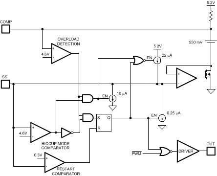 Figure 8. Hiccup Mode Control
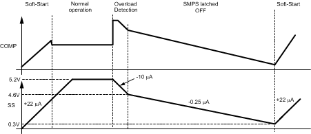 Figure 9. Waveform at SS and COMP Pin due to Continuous Overload
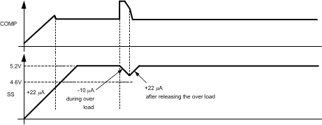 Figure 10. Waveform at SS and COMP Pin due to Brief Overload
7.3.7 Skip Cycle Operation
During light load conditions, the efficiency of the switching power supply typically drops as the losses associated with switching and operating bias currents of the converter become a significant percentage of the power delivered to the load. The largest component of the power loss is the switching loss associated with the gate driver and external MOSFET gate charge. Each PWM cycle consumes a finite amout of energy as the MOSFET is turned on and then turned off. These switching losses are proportional to the frequency of operation. The Skip Cycle function integrated within the LM5021 controller reduces the average switching frequency to reduce switching losses and improve efficiency during light load conditions.
When a light load condition occurs, the COMP pin voltage is reduced by the voltage feedback loop to reduce the peak current delivered by the controller. Referring to Figure 11, the PWM comparator input tracks the COMP pin voltage through a 1.25 V level shift circuit and a 3:1 resistor divider. As the COMP pin voltage falls, the input to the PWM comparator falls proportionately. When the PWM comparator input falls to 125 mV, the Skip Cycle comparator detects the light load condition and disables output pulses from the controller. The controller continues to skip switching cycles until the power supply output falls and the COMP pin voltage increases to demand more output current. The number of cycles skipped will depend on the load and the response time of the frequency compensation network. Eventually the COMP voltage will increase when the voltage loop requires more current to sustain the regulated output voltage. When the PWM comparator input exceeds 130 mV (5 mV hysteresis), normal fixed frequency switching resumes. Typical power supply designs will produce a short burst of output pulses followed by a long skip cycle interval. The average switching frequency in the Skip Cycle mode can be a small fraction of the normal operating frequency of the power supply.
The skip cycle mode of operation can be disabled by adding an offset voltage to the CS pin (refer to Figure 12). A resistive divider connected to a regulated source, injecting a 125 mV offset (minimum) on the CS pin, will force the voltage at the PWM Comparator to be greater than 125 mV, disabling the Skip Cycle Comparator.
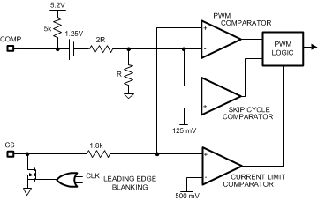 Figure 11. Skip Cycle Control
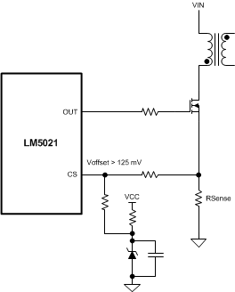 Figure 12. Disabling the Skip Cycle Mode
7.4 Device Functional Modes
7.4.1 Operation With VIN Below 20 V
When a converter is first powered up, there is typically no voltage present on the VIN pin of the controller and the controller is in a low current startup mode. In this mode, there is no activity at the OUT pin and the device is internally in a shutdown mode that consumes minimal current, typically 18 µA. The startup circuit must be capable of supplying the maximum startup current of 25 µA, plus additional current to charge the VIN capacitor to 20 V in any required startup time, at the minimum desired startup voltage for the converter. Once the VIN voltage reaches the startup voltage of 20 V, normal operation in soft start commences. The converter will continue to operate until the VIN voltage falls below the turn off threshold of 7.25 V
7.4.2 Operation in Soft Start
Soft-start mode occurs after the VIN pin reaches the startup voltage after being below 7.25 V or after a hiccup overcurrent cycle. In this mode the reference voltage applied to the PWM comparator from the COMP pin is clamped and allowed to rise at a rate determined by the charging of a capacitor connected to the SS pin. This ramped voltage controls the amount of peak current in the power stage and allows it to increase slowly to reduce stresses on system components. When the clamp level exceeds the level required by the voltage applied to the COMP pin externally, the external feedback circuitry supplying the voltage on COMP assumes control pf the power stage peak current.
7.4.3 Operation Under Normal Conditions
Once the converter has completed soft start, it operates at either a fixed switching frequency with the output pulse width determined by the voltage applied to the COMP pin and the ramp applied to the CS pin, or in a skip cycle mode when the converter load is light. For the normal fixed frequency mode of operation the output is set high when the oscillator starts a new clock cycle (or every other clock cycle in the LM5021-2). The CS pin is connected to the current sensing network for the converter and the voltage on that pin is compared to one-third of the voltage applied to the COMP pin less 1.25 V (see the Functional Block Diagram section) from the external error amplifier and compensation circuit. The CS pin signal should be a linearly increasing ramp proportional to the current in the power stage of the converter. The output pulse terminates when the voltage at the CS pin exceeds one-third of the voltage on COMP less 1.25 V.
7.4.4 Operation in Skip Cycle
During periods of minimal output power demand, the controller will operate in a skip cycle mode to reduce power consumption and increase efficiency at lighter loads. Skip cycle mode is entered when in normal operation the voltage on COMP is reduced by the external error amplifier to the point that the voltage on the PWM comparator falls below 125 mV. This will typically be about 1.625 V or lower at the COMP pin. When this mode is entered, the controller inhibits pulses on the output until the error amplifier and compensation circuit requires approximately 130 mV at the input of the PWM comparator. This is approximately 1.64 V at the COMP pin. The number and frequency of pulses in the skip cycle mode is dependent on the load and response time of the external error amplifier and compensation circuit. Skip cycle operation may be disabled by adding a 125-mV DC offset to the CS pin.
7.4.5 Operation at Overload
If the load on the converter increases beyond design limitations, the converter can fail due to component over stress. The LM5021 uses a fixed maximum CS pin voltage of 500 mV to limit the amount of current in the converter power stage. The output pulse will terminate when the CS pin voltage exceeds this threshold regardless of the current command voltage applied to the COMP pin. For short time duration overload events, the converter will operate normally with typically a small transient drop in output voltage that is corrected by the error amplifier when the overload is removed. If the overload is longer in duration, the error amplifier will apply higher and higher voltage to the COMP pin as the output voltage sags. If the COMP pin voltage exceeds the overload threshold of 4.6 V, the converter will enter hiccup mode.
7.4.6 Operation in Hiccup Mode
If during an overload, the COMP pin voltage rises above 4.6 V, hiccup mode operation is started. In this mode, the OUT pin is held low and the soft start capacitor is discharged using a 10-µA current source. When the soft start capacitor discharges to 0.3 V, a new startup sequence begins with the controller in the soft start mode.