SNVS307G September 2004 – April 2016 LM5010
PRODUCTION DATA.
- 1 Features
- 2 Applications
- 3 Description
- 4 Revision History
- 5 Pin Configuration and Functions
- 6 Specifications
- 7 Detailed Description
- 8 Application and Implementation
- 9 Power Supply Recommendations
- 10Layout
- 11Device and Documentation Support
- 12Mechanical, Packaging, and Orderable Information
封装选项
机械数据 (封装 | 引脚)
散热焊盘机械数据 (封装 | 引脚)
- PWP|14
订购信息
8 Application and Implementation
NOTE
Information in the following applications sections is not part of the TI component specification, and TI does not warrant its accuracy or completeness. TI’s customers are responsible for determining suitability of components for their purposes. Customers should validate and test their design implementation to confirm system functionality.
8.1 Application Information
The LM5010 is a non-synchronous buck regulator converter designed to operate over a wide input voltage and output current range. Spreadsheet-based calculator tools, available on the TI product website at Quick-Start Calculator, can be used to design a single output non-synchronous buck converter.
Alternatively, online WEBENCH® software is available to create a complete buck design and generate the bill of materials, estimated efficiency, solution size, and cost of the complete solution.
8.2 Typical Application
The final circuit is shown in Figure 12, and its performance is shown from Figure 14 to Figure 17.
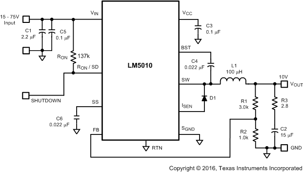 Figure 12. LM5010 Example Circuit
8.2.1 Design Requirements
Table 1 lists the operating parameters for Figure 12.
Table 1. Design Parameters
| PARAMETER | EXAMPLE VALUE |
|---|---|
| Input voltage | 15 V to 75 V |
| Output voltage | 10 V |
| Load current | 150 mA to 1 A |
| Soft-start time | 5 ms |
8.2.2 Detailed Design Procedure
The procedure for calculating the external components is illustrated with a design example. Configure the circuit in Figure 12 according to the components listed in Table 2.
Table 2. List of Components for LM5010 Example Circuit
| COMPONENT | DESCRIPTION | VALUE |
|---|---|---|
| C1 | Ceramic Capacitor | 2.2 µF, 100 V |
| C2 | Ceramic Capacitor | 15 µF, 25 V |
| C3 | Ceramic Capacitor | 0.1 µF, 16 V |
| C4, C6 | Ceramic Capacitor | 0.022 µF, 16 V |
| C5 | Ceramic Capacitor | 0.1 µF, 100 V |
| D1 | Ultra-fast diode | 100 V, 2 A |
| L1 | Inductor | 100 µH |
| R1 | Resistor | 3 kΩ |
| R2 | Resistor | 1 kΩ |
| R3 | Resistor | 2.8 Ω |
| RON | Resistor | 137 kΩ |
| U1 | Switching regulator | — |
8.2.2.1 Component Selection
8.2.2.1.1 R1 and R2
Calculate the ratio of these resistors with Equation 7.
R1 and R2 calculates to 3. The resistors should be chosen from standard value resistors in the range of 1 kΩ to 10 kΩ. Values of 3 kΩ for R1, and 1 kΩ for R2 are used.
8.2.2.1.2 RON, FS
RON sets the ON-time, and can be chosen using Equation 2 to set a nominal frequency, or from Equation 5 if the ON-time at a particular VIN is important. A higher frequency generally means a smaller inductor and capacitors (value, size and cost), but higher switching losses. A lower frequency means a higher efficiency, but with larger components. If PC board space is tight, a higher frequency is better. The resulting ON-time and frequency have a ±25% tolerance, rearranging Equation 2 to Equation 8.

The next larger standard value (137 kΩ) is chosen for RON, yielding a nominal frequency of 618 kHz.
8.2.2.1.3 L1
The inductor value is determined based on the load current, ripple current, and the minimum and maximum input voltage (VIN(min), VIN(max)). See Figure 13.
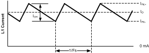 Figure 13. Inductor Current
To keep the circuit in continuous conduction mode, the maximum allowed ripple current is twice the minimum load current, or 300 mAP-P. Using this value of ripple current, the inductor (L1) is calculated using Equation 9 and Equation 10.

where
- FS(min) is the minimum frequency (FS - 25%)

Equation 10 provides the minimum value for inductor L1. When selecting an inductor, use a higher standard value (100 uH). L1 must be rated for the peak current (IPK+) to prevent saturation. The peak current occurs at maximum load current with maximum ripple. The maximum ripple is calculated by rearranging Equation 9 using VIN(max), FS(min), and the minimum inductor value, based on the manufacturer’s tolerance. Assume for Equation 11, Equation 12, and Equation 13 that the inductor’s tolerance is ±20%.


8.2.2.1.4 RCL
Since it is obvious that the lower peak of the inductor current waveform does not exceed 1 A at maximum load current (see Figure 13), it is not necessary to increase the current limit threshold. Therefore RCL is not needed for this exercise. For applications where the lower peak exceeds 1 A, see Increasing The Current Limit Threshold.
8.2.2.1.5 C2 and R3
Since the LM5010 requires a minimum of 25 mVP-P of ripple at the FB pin for proper operation, the required ripple at VOUT1 is increased by R1 and R2. This necessary ripple is created by the inductor ripple current acting on C2’s ESR + R3. First, determine the minimum ripple current with Equation 14.

The minimum ESR for C2 is then equal to Equation 15.

If the capacitor used for C2 does not have sufficient ESR, R3 is added in series as shown in Figure 12. C2 should generally be no smaller than 3.3 µF, although that is dependent on the frequency and the allowable ripple amplitude at VOUT1. Experimentation is usually necessary to determine the minimum value for C2, as the nature of the load may require a larger value. A load which creates significant transients requires a larger value for C2 than a non-varying load.
8.2.2.1.6 D1
The important parameters are reverse recovery time and forward voltage drop. The reverse recovery time determines how long the current surge lasts each time the buck switch is turned on. The forward voltage drop is significant in the event the output is short-circuited as it is mainly this diode’s voltage (plus the voltage across the current limit sense resistor) which forces the inductor current to decrease during the OFF-time. For this reason, a higher voltage is better, although that affects efficiency. A reverse recovery time of ≊30 ns, and a forward voltage drop of ≊0.75 V are preferred. The reverse leakage specification is important as that can significantly affect efficiency. Other types of diodes may have a lower forward voltage drop, but may have longer recovery times, or greater reverse leakage. D1 should be rated for the maximum VIN, and for the peak current when in current limit (IPK in Figure 11) which is equal to Equation 16.
where
- 1.5 A is the maximum guaranteed current limit threshold
- the maximum ripple current was previously calculated as 234 mAP-P
This calculation is only valid when RCL is not required.
8.2.2.1.7 C1
Assuming the voltage supply feeding VIN has a source impedance greater than zero, this capacitor limits the ripple voltage at VIN while supplying most of the switch current during the ON-time. At maximum load current, when the buck switch turns on, the current into VIN increases to the lower peak of the output current waveform, ramps up to the peak value, then drops to zero at turnoff. The average current into VIN during this ON-time is the load current. For a worst case calculation, C1 must supply this average load current during the maximum ON-time. The maximum ON-time is calculated using Equation 5, with a 25% tolerance added in Equation 17.

C1 is calculated with Equation 18.

where
- IO is the load current
- ΔV is the allowable ripple voltage at VIN (1 V for this example)
TI recommends quality ceramic capacitors with a low ESR for C1. To allow for capacitor tolerances and voltage effects, use a 2.2-µF capacitor.
8.2.2.1.8 C3
The capacitor at the VCC pin provides not only noise filtering and stability, but also prevents false triggering of the VCC UVLO at the buck switch ON and OFF transitions. For this reason, C3 should be no smaller than 0.1 µF, and should be a good quality, low ESR, ceramic capacitor. This capacitor also determines the initial start-up delay (t1 in Figure 7).
8.2.2.1.9 C4
TI recommends a value of 0.022 µF for C4. TI recommends a high-quality ceramic capacitor with low ESR, because C4 supplies the surge current to charge the buck switch gate at turnon. A low ESR also ensures a complete recharge during each OFF-time.
8.2.2.1.10 C5
This capacitor suppresses transients and ringing due to long lead inductance at VIN. TI recommends a low ESR, 0.1-µF ceramic chip capacitor, placed physically close to the LM5010.
8.2.2.1.11 C6
The capacitor at the SS pin determines the soft-start time (that is the time for the reference voltage at the regulation comparator and the output voltage), to reach their final value. Determine the time with Equation 19.

For a 5-ms soft-start time, C6 calculates to 0.022 µF.
8.2.2.2 Increasing The Current Limit Threshold
The current limit threshold is nominally 1.25 A, with a minimum guaranteed value of 1 A. If, at maximum load current, the lower peak of the inductor current (IPK– in Figure 13) exceeds 1 A, resistor RCL must be added between SGND and ISEN to increase the current limit threshold to be equal or exceed that lower peak current. This resistor diverts some of the recirculating current from the internal sense resistor so that a higher current level is needed to switch the internal current limit comparator. Calculate IPK– with Equation 20.

where
- IO(max) is the maximum load current
- IOR(min) is the minimum ripple current calculated using Equation 14
RCL is calculated with Equation 21.

where
- 0.11 Ω is the minimum value of the internal resistance from SGND to ISEN
The next smaller standard value resistor should be used for RCL. With the addition of RCL it is necessary to check the average and peak current values to ensure they do not exceed the LM5010 limits. At maximum load current the average current through the internal sense resistor is calculated with Equation 22.

If IAVE is less than 2 A, no changes are necessary. If it exceeds 2 A, RCL must be reduced. The upper peak of the inductor current (IPK+), at maximum load current, is calculated using Equation 23.

where
- IOR(max) is calculated using Equation 11
If IPK+ exceeds 3.5 A , the inductor value must be increased to reduce the ripple amplitude. This necessitates recalculation of IOR(min), IPK–, and RCL.
When the circuit is in current limit, the upper peak current out of the SW pin is calculated with Equation 24.

The inductor L1 and diode D1 must be rated for this current.
8.2.2.3 Ripple Configuration
The LM5010 uses a constant-ON-time (COT) control scheme where the ON-time is terminated by a one-shot and the OFF-time is terminated by the feedback voltage (VFB) falling below the reference voltage. Therefore, for stable operation, the feedback voltage must decrease monotonically in phase with the inductor current during the OFF-time. Furthermore, this change in feedback voltage (VFB) during OFF-time must be large enough to dominate any noise present at the feedback node.
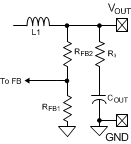
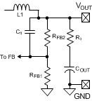
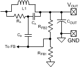
Table 3 presents three different methods for generating appropriate voltage ripple at the feedback node. Type 1 and type 2 ripple circuits couple the ripple from the output of the converter to the feedback node (FB). The output voltage ripple has two components:
- Capacitive ripple caused by the inductor current ripple charging or discharging the output capacitor.
- Resistive ripple caused by the inductor current ripple flowing through the ESR of the output capacitor and R3.
Table 3. Ripple Configuration
| TYPE 1 | TYPE 2 | TYPE 3 |
|---|---|---|
| Lowest cost | Reduced ripple | Minimum ripple |
 |
 |
 |
|
Equation 25.
 |
Equation 26.
 |
Equation 27.
 |
The capacitive ripple is out of phase with the inductor current. As a result, the capacitive ripple does not decrease monotonically during the OFF-time. The resistive ripple is in phase with the inductor current and decreases monotonically during the OFF-time. The resistive ripple must exceed the capacitive ripple at output (VOUT) for stable operation. If this condition is not satisfied, then unstable switching behavior is observed in COT converters with multiple ON-time bursts in close succession followed by a long OFF-time.
The type 3 ripple method uses a ripple injection circuit with RA, CA, and the switch node (SW) voltage to generate a triangular ramp. This triangular ramp is then AC-coupled into the feedback node (FB) using the capacitor CB. This circuit is suited for applications where low output voltage ripple is imperative because this circuit does not use the output voltage ripple. See AN-1481 Controlling Output Ripple and Achieving ESR Independence in Constant ON-Time (COT) Regulator Designs, (SNVA166) for more details on each ripple generation method.
8.2.3 Application Curves
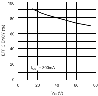 Figure 14. Efficiency vs VIN
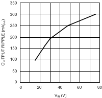 Figure 16. Output Voltage Ripple vs VIN
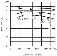 Figure 15. Efficiency vs Load Current and VIN
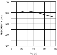 Figure 17. Frequency vs VIN
8.3 Do's and Don'ts
A minimum load current of 1 mA is required to maintain proper operation. If the load current falls below that level, the bootstrap capacitor can discharge during the long OFF-time and the circuit either shuts down or cycles ON and OFF at a low frequency. If the load current is expected to drop below 1 mA in the application, choose the feedback resistors to be low enough in value to provide the minimum required current at nominal VOUT.