ZHCSEM6A February 2016 – February 2016 LM36923H
PRODUCTION DATA.
- 1 特性
- 2 应用
- 3 说明
- 4 修订历史记录
- 5 Pin Configuration and Functions
- 6 Specifications
-
7 Detailed Description
- 7.1 Overview
- 7.2 Functional Block Diagram
- 7.3 Feature Description
- 7.4
Device Functional Modes
- 7.4.1 Brightness Control Modes
- 7.4.2 Boost Switching Frequency
- 7.4.3 Auto-Switching Frequency
- 7.4.4 I2C Address Select (ASEL)
- 7.4.5
Fault Protection/Detection
- 7.4.5.1
Overvoltage Protection (OVP)
- 7.4.5.1.1 Case 1 OVP Fault Only (OVP Threshold Hit and All Enabled Current Sink Inputs > 40 mV)
- 7.4.5.1.2 Case 2a OVP Fault and Open LED String Fault (OVP Threshold Occurrence and Any Enabled Current Sink Input ≤ 40 mV)
- 7.4.5.1.3 Case 2b OVP Fault and Open LED String Fault (OVP Threshold Duration and Any Enabled Current Sink Input ≤ 40 mV)
- 7.4.5.1.4 OVP/LED Open Fault Shutdown
- 7.4.5.1.5 Testing for LED String Open
- 7.4.5.2 Voltage Limitations on LED1, LED2, and LED3
- 7.4.5.3 LED String Short Fault
- 7.4.5.4 Overcurrent Protection (OCP)
- 7.4.5.5 Device Overtemperature
- 7.4.5.1
Overvoltage Protection (OVP)
- 7.5 Programming
- 7.6 Register Maps
- 8 Applications and Implementation
- 9 Power Supply Recommendations
- 10Layout
- 11器件和文档支持
- 12机械、封装和可订购信息
8 Applications and Implementation
NOTE
Information in the following applications sections is not part of the TI component specification, and TI does not warrant its accuracy or completeness. TI’s customers are responsible for determining suitability of components for their purposes. Customers should validate and test their design implementation to confirm system functionality.
8.1 Application Information
The LM36923H provides a complete high-performance LED lighting solution for mobile handsets. The LM36923H is highly configurable and can support multiple LED configurations.
8.2 Typical Application
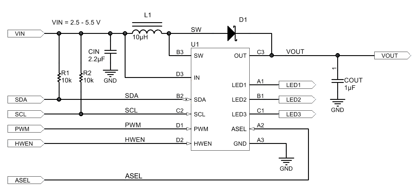 Figure 30. LM36923H Typical Application
8.2.1 Design Requirements
| DESIGN PARAMETER | EXAMPLE VALUE |
|---|---|
| Minimum input voltage (VIN) | 2.7 V |
| LED parallel/series configuration | 3 × 5 |
| LED maximum forward voltage (Vƒ) | 3.2 V |
| Efficiency | 82% |
The number of LED strings, number of series LEDs, and minimum input voltage are needed in order to calculate the peak input current. This information guides the designer to make the appropriate inductor selection for the application. The LM36923H boost converter output voltage (VOUT) is calculated: number of series LEDs × Vƒ + 0.23 V. The LM36923H boost converter output current (IOUT) is calculated: number of parallel LED strings × 25 mA. The LM36923H peak input current is calculated using Equation 5.
8.2.2 Detailed Design Procedure
Table 20. Typical Application Component List
| CONFIGURATION | L1 | D1 | COUT | |
|---|---|---|---|---|
| 3p7s, 3p8s | VLF504012MT-100M VLF504012MT-150M |
NSR0530P2T5G | C2012X7R1H105K085AC | |
| 3p6s | VLF504012MT-220M | NSR0530P2T5G | C2012X7R1H105K085AC | |
| 3p5s | VLF403210MT-100M | NSR0530P2T5G | C2012X7R1H105K085AC | |
| 3p4s | VLF302510MT-100M | NSR0530P2T5G | C2012X7R1H105K085AC | |
8.2.2.1 Component Selection
8.2.2.1.1 Inductor
The LM36923H requires a typical inductance in the range of 4.7 µH to 10 µH. When selecting the inductor, ensure that the saturation rating for the inductor is high enough to accommodate the peak inductor current of the application (IPEAK) given in the inductor datasheet. The peak inductor current occurs at the maximum load current, the maximum output voltage, the minimum input voltage, and the minimum switching frequency setting. Also, the peak current requirement increases with decreasing efficiency. IPEAK can be estimated using Equation 5:

Also, the peak current calculated above is different from the peak inductor current setting (ISAT). The NMOS switch current limit setting (ICL_MIN) must be greater than IPEAK from Equation 5 above.
8.2.2.1.2 Output Capacitor
The LM36923H requires a ceramic capacitor with a minimum of 0.4 µF of capacitance at the output, specified over the entire range of operation. This ensures that the device remains stable and oscillation free. The 0.4 µF of capacitance is the minimum amount of capacitance, which is different than the value of capacitor. Capacitance would take into account tolerance, temperature, and DC voltage shift.
Table 21 lists possible output capacitors that can be used with the LM36923H. Figure 31 shows the DC bias of the four TDK capacitors. The useful voltage range is determined from the effective output voltage range for a given capacitor as determined by Equation 6:

Table 21. Recommended Output Capacitors
| PART NUMBER | MANUFACTURER | CASE SIZE | VOLTAGE RATING (V) | NOMINAL CAPACITANCE (µF) | TOLERANCE (%) | TEMPERATURE COEFFICIENT (%) | RECOMMENDED MAX OUTPUT VOLTAGE (FOR SINGLE CAPACITOR) |
|---|---|---|---|---|---|---|---|
| C2012X5R1H105K085AB | TDK | 0805 | 50 | 1 | ±10 | ±15 | 22 |
| C2012X5R1H225K085AB | TDK | 0805 | 50 | 2.2 | ±10 | ±15 | 24 |
| C1608X5R1V225K080AC | TDK | 0603 | 35 | 2.2 | ±10 | ±15 | 12 |
| C1608X5R1H105K080AB | TDK | 0603 | 50 | 1 | ±10 | ±15 | 15 |
For example, with a 10% tolerance, and a 15% temperature coefficient, the DC voltage derating must be ≥ 0.38 / (0.9 × 0.85) = 0.5 µF. For the C1608X5R1H225K080AB (0603, 50-V) device, the useful voltage range occurs up to the point where the DC bias derating falls below 0.523 µF, or around 12 V. For configurations where VOUT is > 15 V, two of these capacitors can be paralleled, or a larger capacitor such as the C2012X5R1H105K085AB must be used.
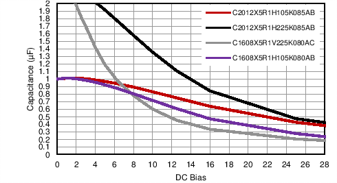 Figure 31. DC Bias Derating for 0805 Case Size and
0603 Case Size 35-V and 50-V Ceramic Capacitors
8.2.2.1.3 Input Capacitor
The input capacitor in a boost is not as critical as the output capacitor. The input capacitor primary function is to filter the switching supply currents at the device input and to filter the inductor current ripple at the input of the inductor. The recommended input capacitor is a 2.2-µF ceramic (0402, 10-V device) or equivalent.
8.2.3 Application Curves
L1 = 4.7 µH (VLF504012-4R7M) or 10 µH (VLF504015-100M) as noted in graphs, D1 = NSR240P2T5G, LEDs are Samsung SPMWHT325AD5YBTMS0, temperature = 25°C, VIN = 3.7 V, unless otherwise noted.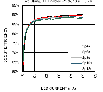 Figure 32. Boost Efficiency vs Series LEDs
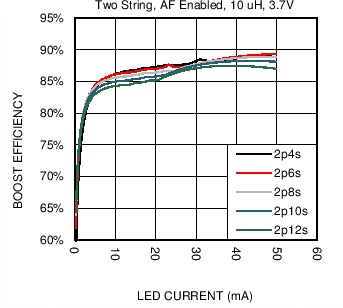 Figure 34. Boost Efficiency vs Series LEDs
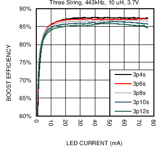 Figure 36. Boost Efficiency vs Series LEDs
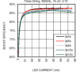 Figure 38. Boost Efficiency vs Series LEDs
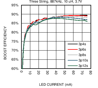 Figure 40. Boost Efficiency vs Series LEDs
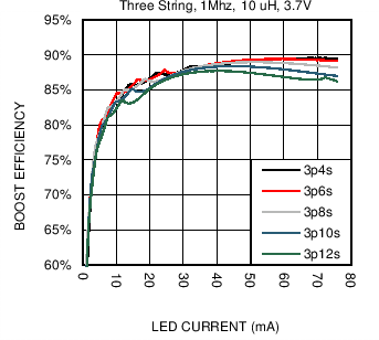 Figure 42. Boost Efficiency vs Series LEDs
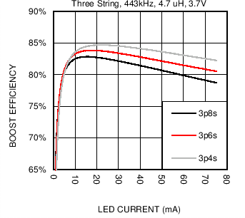 Figure 44. Boost Efficiency vs Series LEDs
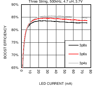 Figure 46. Boost Efficiency vs Series LEDs
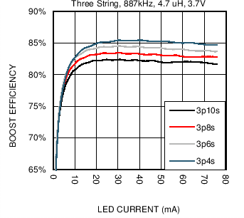 Figure 48. Boost Efficiency vs Series LEDs
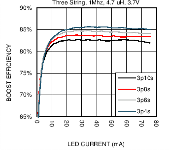 Figure 50. Boost Efficiency vs Series LEDs
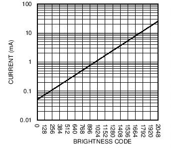 Figure 52. LED Current vs Brightness Code (Exponential Mapping)
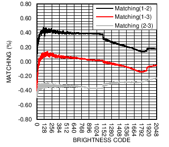 Figure 54. LED Matching (Exponential Mapping)
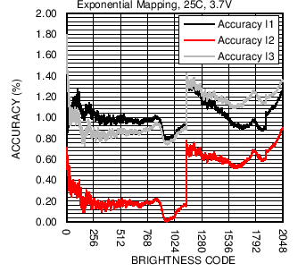 Figure 56. LED Current Accuracy
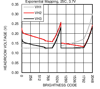 Figure 58. LED Headroom Voltage (Mis-Matched Strings)
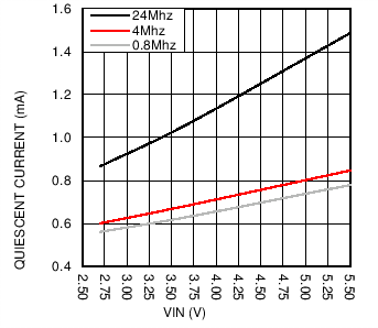 Figure 60. Current vs PWM Sample Frequency
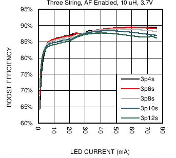 Figure 33. Boost Efficiency vs Series LEDs
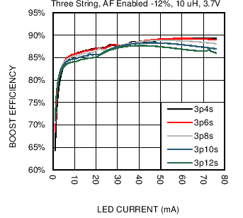 Figure 35. Boost Efficiency vs Series LEDs
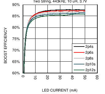 Figure 37. Boost Efficiency vs Series LEDs
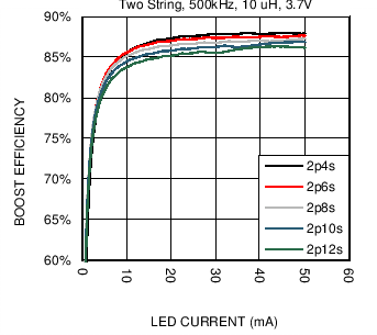 Figure 39. Boost Efficiency vs Series LEDs
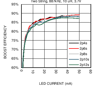 Figure 41. Boost Efficiency vs Series LEDs
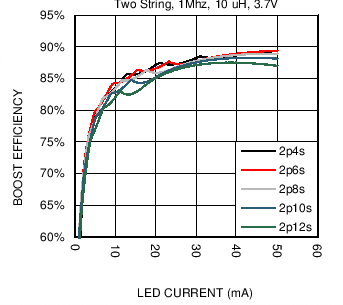 Figure 43. Boost Efficiency vs Series LEDs
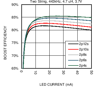 Figure 45. Boost Efficiency vs Series LEDs
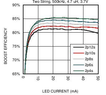 Figure 47. Boost Efficiency vs Series LEDs
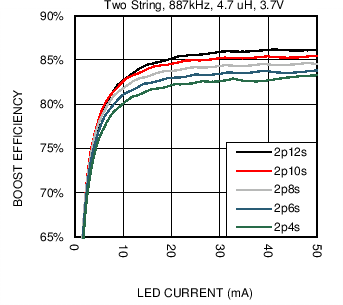 Figure 49. Boost Efficiency vs Series LEDs
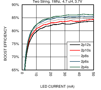 Figure 51. Boost Efficiency vs Series LEDs
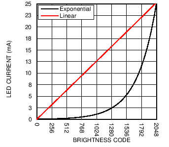 Figure 53. LED Current vs Brightness Code
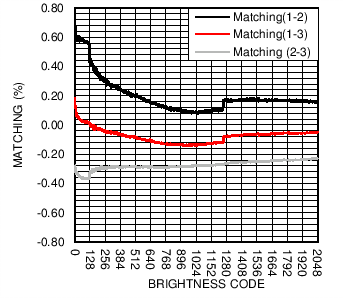 Figure 55. LED Matching (Linear Mapping)
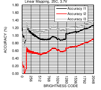 Figure 57. LED Current Accuracy
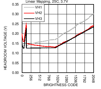 Figure 59. LED Headroom Voltage (Mis-Matched Strings)