ZHCSEM6A February 2016 – February 2016 LM36923H
PRODUCTION DATA.
- 1 特性
- 2 应用
- 3 说明
- 4 修订历史记录
- 5 Pin Configuration and Functions
- 6 Specifications
-
7 Detailed Description
- 7.1 Overview
- 7.2 Functional Block Diagram
- 7.3 Feature Description
- 7.4
Device Functional Modes
- 7.4.1 Brightness Control Modes
- 7.4.2 Boost Switching Frequency
- 7.4.3 Auto-Switching Frequency
- 7.4.4 I2C Address Select (ASEL)
- 7.4.5
Fault Protection/Detection
- 7.4.5.1
Overvoltage Protection (OVP)
- 7.4.5.1.1 Case 1 OVP Fault Only (OVP Threshold Hit and All Enabled Current Sink Inputs > 40 mV)
- 7.4.5.1.2 Case 2a OVP Fault and Open LED String Fault (OVP Threshold Occurrence and Any Enabled Current Sink Input ≤ 40 mV)
- 7.4.5.1.3 Case 2b OVP Fault and Open LED String Fault (OVP Threshold Duration and Any Enabled Current Sink Input ≤ 40 mV)
- 7.4.5.1.4 OVP/LED Open Fault Shutdown
- 7.4.5.1.5 Testing for LED String Open
- 7.4.5.2 Voltage Limitations on LED1, LED2, and LED3
- 7.4.5.3 LED String Short Fault
- 7.4.5.4 Overcurrent Protection (OCP)
- 7.4.5.5 Device Overtemperature
- 7.4.5.1
Overvoltage Protection (OVP)
- 7.5 Programming
- 7.6 Register Maps
- 8 Applications and Implementation
- 9 Power Supply Recommendations
- 10Layout
- 11器件和文档支持
- 12机械、封装和可订购信息
6 Specifications
6.1 Absolute Maximum Ratings
over operating free-air temperature range (unless otherwise noted)(1)| MIN | MAX | UNIT | ||
|---|---|---|---|---|
| IN | Input voltage | –0.3 | 6 | V |
| OUT | Output overvoltage sense input | –0.3 | 40 | V |
| SW | Inductor connection | –0.3 | 40 | V |
| LED1, LED2, LED3 | LED string cathode connection | –0.3 | 30 | V |
| HWEN, PWM, SDA, SCL, ASEL | Logic I/Os | –0.3 | 6 | V |
| Maximum junction temperature, TJ_MAX | 150 | °C | ||
| Storage temperature, Tstg | –65 | 150 | °C | |
(1) Stresses beyond those listed under Absolute Maximum Ratings may cause permanent damage to the device. These are stress ratings only, which do not imply functional operation of the device at these or any other conditions beyond those indicated under Recommended Operating Conditions. Exposure to absolute-maximum-rated conditions for extended periods may affect device reliability.
6.2 ESD Ratings
| VALUE | UNIT | |||
|---|---|---|---|---|
| V(ESD) | Electrostatic discharge | Human-body model (HBM), per ANSI/ESDA/JEDEC JS-001(1) | ±2000 | V |
| Charged-device model (CDM), per JEDEC specification JESD22-C101(2) | ±500 | |||
(1) JEDEC document JEP155 states that 500-V HBM allows safe manufacturing with a standard ESD control process. Pins listed as ±2000 V may actually have higher performance.
(2) JEDEC document JEP157 states that 250-V CDM allows safe manufacturing with a standard ESD control process. Pins listed as ±500 V may actually have higher performance.
6.3 Recommended Operating Conditions
over operating free-air temperature range (unless otherwise noted)| MIN | MAX | UNIT | ||
|---|---|---|---|---|
| IN | Input voltage | 2.5 | 5.5 | V |
| OUT | Overvoltage sense input | 0 | 38 | V |
| SW | Inductor connection | 0 | 38 | V |
| LED1, LED2, LED3 | LED string cathode connection | 0 | 29.5 | V |
| HWEN, PWM, SDA, SCL, ASEL | Logic I/Os | 0 | 5.5 | V |
6.4 Thermal Information
| THERMAL METRIC(1) | LM36923H | UNIT | |
|---|---|---|---|
| YFQ (DSBGA) | |||
| 12 PINS | |||
| RθJA | Junction-to-ambient thermal resistance | 88.9 | °C/W |
| RθJC(top) | Junction-to-case (top) thermal resistance | 0.7 | °C/W |
| RθJB | Junction-to-board thermal resistance | 43.9 | °C/W |
| ΨθJT | Junction-to-top characterization parameter | 2.9 | °C/W |
| ΨθJB | Junction-to-board characterization parameter | 43.7 | °C/W |
(1) For more information about traditional and new thermal metrics, see the Semiconductor and IC Package Thermal Metrics application report, SPRA953.
6.5 Electrical Characteristics
Minimum and maximum limits apply over the full operating ambient temperature range (−40°C ≤ TA ≤ 85°C), typical values are at TA = 25°C, and VIN = 3.6 V (unless otherwise noted).| PARAMETER | TEST CONDITIONS | MIN | TYP | MAX | UNIT | ||
|---|---|---|---|---|---|---|---|
| BOOST | |||||||
| IMATCH(1) | LED current matching ILED1 to ILED2 to ILED3 | 50 µA ≤ ILED ≤ 25 mA, 2.7 V ≤ VIN ≤ 5 V (linear or exponential mode) | –1% | 0.1% | 1% | ||
| Accuracy | Absolute accuracy (ILED1, ILED2, ILED3) | 50 µA ≤ ILED ≤ 25 mA, 2.7 V ≤ VIN ≤ 5 V (linear or exponential mode) | –3% | 0.1% | 3% | ||
| ILED_MIN | Minimum LED current (per string) | PWM or I2C current control (linear or exponential mode) | 50 | µA | |||
| ILED_MAX | Maximum LED current (per string) | 25 | mA | ||||
| RDNL | IDAC ratio-metric DNL | exponential mode only | 1/3 (0.3%) |
LSB | |||
| VHR | Regulated current sink headroom voltage | ILED = 25 mA | 210 | mV | |||
| ILED = 5 mA | 100 | ||||||
| VHR_MIN | Current sink minimum headroom voltage | ILED = 95% of nominal, ILED = 5 mA | 35 | 50 | mV | ||
| Efficiency | Typical efficiency | VIN = 3.7 V, ILED = 5 mA/string, Typical Application circuit (3x7 LEDs), (POUT/PIN) | 87% | ||||
| RNMOS | NMOS switch on resistance | ISW = 250 mA | 0.29 | Ω | |||
| ICL | NMOS switch current limit | 2.7 V ≤ VIN ≤ 5 V | OCP = 00 | 575 | 750 | 875 | mA |
| OCP = 01 | 860 | 1000 | 1110 | ||||
| OCP = 10 | 1100 | 1250 | 1400 | ||||
| OCP = 11 | 1350 | 1500 | 1650 | ||||
| VOVP | Output overvoltage protection | ON threshold, 2.7 V ≤ VIN ≤ 5 V | OVP = 00 | 16 | 17 | 17.5 | V |
| OVP = 01 | 23 | 24 | 25 | ||||
| OVP = 10 | 30 | 31 | 32 | ||||
| OVP = 11 | 37 | 38 | 39 | ||||
| OVP Hysteresis | 0.5 | V | |||||
| ƒSW | Switching frequency | 2.7 V ≤ VIN ≤ 5 V, boost frequency shift = 0 |
Boost frequency select = 0 | 475 | 500 | 525 | kHz |
| Boost frequency select = 1 | 950 | 1000 | 1050 | ||||
| DMAX | Maximum boost duty cycle | 92% | 94% | ||||
| ISHDN | Shutdown current | Chip enable bit = 0, SDA = SCL = IN or GND, 2.7 V ≤ VIN ≤ 5 V | 1.2 | 5 | µA | ||
| TSD | Thermal shutdown | 135 | °C | ||||
| Hysteresis | 15 | ||||||
| PWM INPUT | |||||||
| Min ƒPWM | 50 | Hz | |||||
| Max ƒPWM | Sample rate = 24 MHz | 50 | kHz | ||||
| tMIN_ON | Minimum pulse ON time | Sample rate = 24 MHz | 183.3 | ns | |||
| Sample rate = 4 MHz | 1100 | ||||||
| Sample rate = 800 kHz | 5500 | ||||||
| tMIN_OFF | Minimum pulse OFF time | Sample rate = 24 MHz | 183.3 | ns | |||
| Sample rate = 4 MHz | 1100 | ||||||
| Sample rate = 800 kHz | 5500 | ||||||
| tSTART-UP | Turnon delay from shutdown to backlight on | PWM input active, PWM = logic high,HWEN input from low to high, ƒPWM = 10 kHz (50% duty cycle) | 3.5 | 5 | ms | ||
| PWMRES | PWM input resolution | 1.6 kHz ≤ ƒPWM ≤ 12 kHz, PWM hysteresis = 00, PWM sample rate = 11 | 11 | bits | |||
| VIH | Input logic high | HWEN, ASEL, SCL, SDA, PWM inputs | 1.25 | VIN | V | ||
| VIL | Input logic low | HWEN, ASEL, SCL, SDA, PWM inputs | 0 | 0.4 | |||
| tGLITCH | PWM input glitch rejection | PWM pulse filter = 00 | 0 | 15 | ns | ||
| PWM pulse filter = 01 | 60 | 100 | 140 | ||||
| PWM pulse filter = 10 | 90 | 150 | 210 | ||||
| PWM pulse filter = 11 | 120 | 200 | 280 | ||||
| tPWM_STBY | PWM shutdown period | Sample rate = 24 MHz | 0.54 | 0.6 | 0.66 | ms | |
| Sample rate = 4 MHz | 2.7 | 3 | 3.3 | ||||
| Sample rate = 800 kHz | 22.5 | 25 | 27.5 | ||||
(1) LED Current Matching between strings is given as the worst case matching between any two strings. Matching is calculated as ((ILEDX – ILEDY)/(ILEDX + ILEDY)) × 100.
6.6 I2C Timing Requirements
See Figure 1| MIN | MAX | UNIT | ||
|---|---|---|---|---|
| t1 | SCL clock period | 2.5 | µs | |
| t2 | Data in setup time to SCL high | 100 | ns | |
| t3 | Data out stable after SCL low | 0 | ns | |
| t4 | SDA low Setup Time to SCL low (start) | 100 | ns | |
| t5 | SDA high hold time after SCL high (stop) | 100 | ns | |
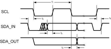 Figure 1. I2C Timing
6.7 Typical Characteristics
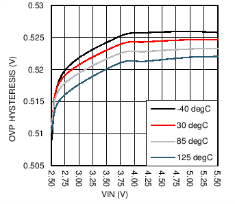
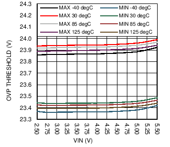
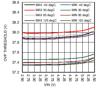
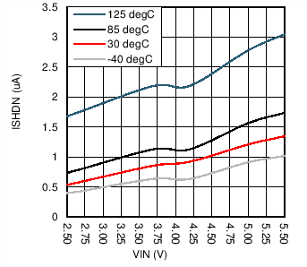
| HWEN = GND |
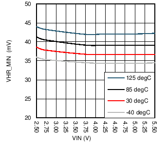
| ILED = 5 mA |
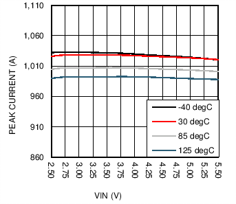
| Open Loop |
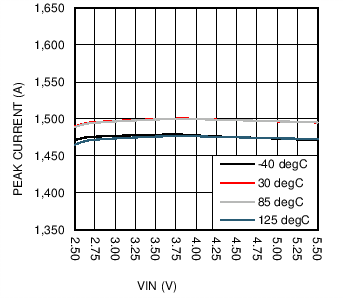
| Open Loop |
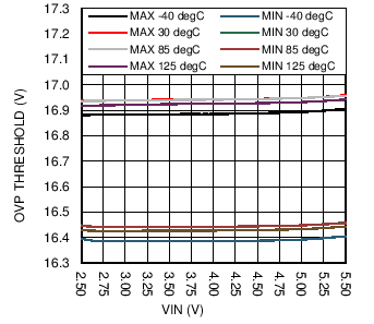
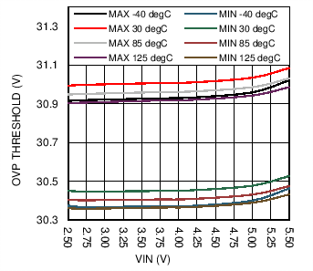
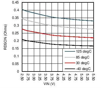
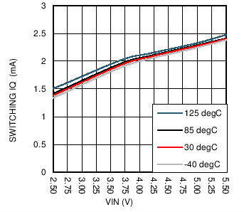
| fSW= 1 Mhz | No Load |
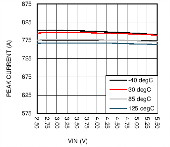
| Open Loop |
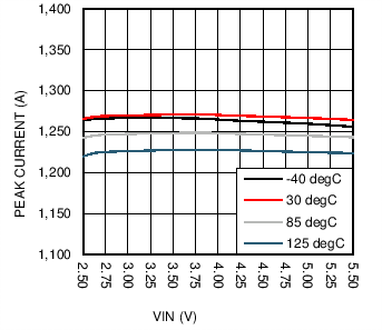
| Open Loop |