ZHCSGN9D February   2016  – March 2018 LM36274

PRODUCTION DATA.  

  1. 特性
  2. 应用
    1.     简化原理图
  3. 说明
    1.     背光效率,4P6S
  4. 修订历史记录
  5. Pin Configuration and Functions
    1.     Pin Functions
  6. Specifications
    1. 6.1 Absolute Maximum Ratings
    2. 6.2 ESD Ratings
    3. 6.3 Recommended Operating Conditions
    4. 6.4 Thermal Information
    5. 6.5 Electrical Characteristics
    6. 6.6 I2C Timing Requirements (Fast Mode)
    7. 6.7 Typical Characteristics
  7. Detailed Description
    1. 7.1 Overview
    2. 7.2 Functional Block Diagram
    3. 7.3 Features Description
      1. 7.3.1 Enabling the LM36274
      2. 7.3.2 Backlight
        1. 7.3.2.1 Current Sink Enable
        2. 7.3.2.2 Brightness Mapping
          1. 7.3.2.2.1 Linear Mapping
          2. 7.3.2.2.2 Exponential Mapping
        3. 7.3.2.3 Backlight Brightness Control Modes
          1. 7.3.2.3.1 I2C Brightness Control (PWM Pin Disabled)
          2. 7.3.2.3.2 I2C × PWM Brightness Control (PWM Pin Enabled)
            1. 7.3.2.3.2.1 PWM Ramper
        4. 7.3.2.4 Boost Switching Frequency
          1. 7.3.2.4.1 Minimum Inductor Select
        5. 7.3.2.5 Boost Feedback Gain Select
        6. 7.3.2.6 Auto Switching Frequency
        7. 7.3.2.7 PWM Input
          1. 7.3.2.7.1 PWM Sample Frequency
            1. 7.3.2.7.1.1 PWM Resolution and Input Frequency Range
            2. 7.3.2.7.1.2 PWM Sample Rate and Efficiency
              1. 7.3.2.7.1.2.1 PWM Sample Rate Example
          2. 7.3.2.7.2 PWM Hysteresis
          3. 7.3.2.7.3 PWM Step Response
          4. 7.3.2.7.4 PWM Timeout
          5. 7.3.2.7.5 PWM-to-Digital Code Readback
        8. 7.3.2.8 Regulated Headroom Voltage
        9. 7.3.2.9 Backlight Fault Protection and Faults
          1. 7.3.2.9.1 Backlight Overvoltage Protection (OVP)
          2. 7.3.2.9.2 Backlight Overcurrent Protection (OCP)
      3. 7.3.3 LCM Bias
        1. 7.3.3.1 Display Bias Boost Converter (VVPOS, VVNEG)
        2. 7.3.3.2 Auto Sequence Mode
        3. 7.3.3.3 Wake-up Mode
          1. 7.3.3.3.1 Wake1 Mode
          2. 7.3.3.3.2 Wake2 Mode
        4. 7.3.3.4 Active Discharge
        5. 7.3.3.5 LCM Bias Protection and Faults
          1. 7.3.3.5.1 LCM Overvoltage (OVP) Protection
          2. 7.3.3.5.2 VPOS Short-Circuit Protection
          3. 7.3.3.5.3 VNEG Short-Circuit Protection
      4. 7.3.4 Software Reset
      5. 7.3.5 HWEN Input
      6. 7.3.6 Thermal Shutdown (TSD)
    4. 7.4 Device Functional Modes
      1. 7.4.1 Modes of Operation
    5. 7.5 Programming
      1. 7.5.1 I2C-Compatible Serial Bus Interface
        1. 7.5.1.1 Interface Bus Overview
        2. 7.5.1.2 Data Transactions
        3. 7.5.1.3 Acknowledge Cycle
        4. 7.5.1.4 Acknowledge After Every Byte Rule
        5. 7.5.1.5 Addressing Transfer Formats
        6. 7.5.1.6 Register Programming
    6. 7.6 Register Maps
      1. 7.6.1  Revision Register (Address = 0x01)[Reset = 0x01]
        1. Table 11. Revision Register Field Descriptions
      2. 7.6.2  Backlight Configuration1 Register (Address = 0x02)[Reset = 0x28]
        1. Table 12. Backlight Configuration 1 Register Field Descriptions
      3. 7.6.3  Backlight Configuration 2 Register (Address = 0x03)[Reset = 0x8D]
        1. Table 13. Backlight Configuration 2 Register Field Descriptions
      4. 7.6.4  Backlight Brightness LSB Register (Address = 0x04)[Reset = 0x07]
        1. Table 14. Backlight Brightness LSB Register Field Descriptions
      5. 7.6.5  Backlight Brightness MSB Register (Address = 0x05)[Reset = 0xFF]
        1. Table 15. Backlight Brightness MSB Register Field Descriptions
      6. 7.6.6  Backlight Auto-Frequency Low Threshold Register (Address = 0x06)[Reset = 0x00]
        1. Table 16. Backlight Auto-Frequency Low Threshold Field Descriptions
      7. 7.6.7  Backlight Auto-Frequency High Threshold Register (Address = 0x07)[Reset = 0x00]
        1. Table 17. Backlight Auto-Frequency High Threshold Field Descriptions
      8. 7.6.8  Backlight Enable Register (Address = 0x08)[Reset = 0x00]
        1. Table 18. Backlight Enable Register Field Descriptions
      9. 7.6.9  Bias Configuration 1 Register (Address = 0x09)[Reset = 0x18]
        1. Table 19. Bias Configuration 1 Register Field Descriptions
      10. 7.6.10 Bias Configuration 2 register (Address = 0x0A)[Reset = 0x11]
        1. Table 20. Bias Configuration 2 Register Field Descriptions
      11. 7.6.11 Bias Configuration 3 Register (Address = 0x0B)[Reset = 0x00]
        1. Table 21. Bias Configuration 3 Register Field Descriptions
      12. 7.6.12 LCM Boost Bias Register (Address = 0x0C)[Reset = 0x28]
        1. Table 22. LCM Boost Bias Register Field Descriptions
      13. 7.6.13 VPOS Bias Register (Address = 0x0D)[Reset = 0x1E]
        1. Table 23. VPOS Bias Register Field Descriptions
      14. 7.6.14 VNEG Bias Register (Address = 0x0E)[Reset = 0x1C]
        1. Table 24. VNEG Bias Register Field Descriptions
      15. 7.6.15 Flags Register (Address = 0x0F)[Reset = 0x00]
        1. Table 25. Flags Register Field Descriptions
      16. 7.6.16 Option 1 Register (Address = 0x10)[Reset = 0x06]
        1. Table 26. Option 1 Register Field Descriptions
      17. 7.6.17 Option 2 Register (Address = 0x11)[Reset = 0x35]
        1. Table 27. Option 2 Register Field Descriptions
      18. 7.6.18 PWM-to-Digital Code Readback LSB Register (Address = 0x12)[Reset = 0x00]
        1. Table 28. PWM-to-Digital Code Readback LSB Register Field Descriptions
      19. 7.6.19 PWM-to-Digital Code Readback MSB Register (Address = 0x13)[Reset = 0x00]
        1. Table 29. PWM-to-Digital Code Readback MSB Register Field Descriptions
  8. Application and Implementation
    1. 8.1 Application Information
    2. 8.2 Typical Application
      1. 8.2.1 Design Requirements
      2. 8.2.2 Detailed Design Procedure
        1. 8.2.2.1 Component Selection
          1. 8.2.2.1.1 Inductor Selection
          2. 8.2.2.1.2 Boost Output Capacitor Selection
          3. 8.2.2.1.3 Input Capacitor Selection
      3. 8.2.3 Application Curves
        1. 8.2.3.1 Backlight Curves
          1. 8.2.3.1.1 Two LED Strings
          2. 8.2.3.1.2 Three LED Strings
          3. 8.2.3.1.3 Four LED Strings
        2. 8.2.3.2 LCM Bias Curves
  9. Power Supply Recommendations
  10. 10Layout
    1. 10.1 Layout Guidelines
    2. 10.2 Layout Example
  11. 11器件和文档支持
    1. 11.1 器件支持
      1. 11.1.1 第三方产品免责声明
      2. 11.1.2 开发支持
    2. 11.2 文档支持
      1. 11.2.1 相关文档
    3. 11.3 接收文档更新通知
    4. 11.4 社区资源
    5. 11.5 商标
    6. 11.6 静电放电警告
    7. 11.7 Glossary
  12. 12机械、封装和可订购信息

封装选项

机械数据 (封装 | 引脚)
散热焊盘机械数据 (封装 | 引脚)
订购信息

Data Transactions

One data bit is transferred during each clock pulse. Data is sampled during the high state of the SCL. Consequently, throughout the clock’s high period, the data remains stable. Any changes on the SDA line during the high state of the SCL and in the middle of a transaction, aborts the current transaction. New data is sent during the low SCL state. This protocol permits a single data line to transfer both command/control information and data using the synchronous serial clock.
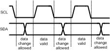
LM36274 I2C_Data_Validity.gifFigure 42. Data Validity

Each data transaction is composed of a start condition, a number of byte transfers (set by the software), and a stop condition to terminate the transaction. Every byte written to the SDA bus must be 8 bits long and is transferred with the most significant bit first. After each byte, an acknowledge signal must follow. The following sections provide further details of this process.
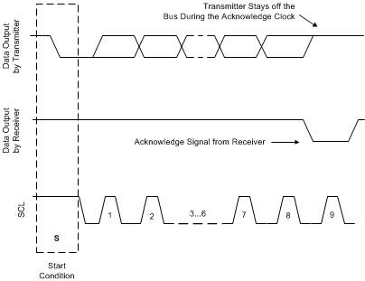
LM36274 I2C_Acknowledge.gifFigure 43. Acknowledge Signal

The Master device on the bus always generates the start and stop conditions (control codes). After a Start Condition is generated, the bus is considered busy, and it retains this status until a certain time after a stop condition is generated. A high-to-low transition of the data line (SDA) while the clock (SCL) is high indicates a start condition. A low-to-high transition of the SDA line while the SCL is high indicates a stop condition.

LM36274 I2C_Start_Stop.gifFigure 44. Start and Stop Conditions

In addition to the first start condition, a repeated start condition can be generated in the middle of a transaction. This allows another device to be accessed, or a register read cycle.