ZHCSGN9D February   2016  – March 2018 LM36274

PRODUCTION DATA.  

  1. 特性
  2. 应用
    1.     简化原理图
  3. 说明
    1.     背光效率,4P6S
  4. 修订历史记录
  5. Pin Configuration and Functions
    1.     Pin Functions
  6. Specifications
    1. 6.1 Absolute Maximum Ratings
    2. 6.2 ESD Ratings
    3. 6.3 Recommended Operating Conditions
    4. 6.4 Thermal Information
    5. 6.5 Electrical Characteristics
    6. 6.6 I2C Timing Requirements (Fast Mode)
    7. 6.7 Typical Characteristics
  7. Detailed Description
    1. 7.1 Overview
    2. 7.2 Functional Block Diagram
    3. 7.3 Features Description
      1. 7.3.1 Enabling the LM36274
      2. 7.3.2 Backlight
        1. 7.3.2.1 Current Sink Enable
        2. 7.3.2.2 Brightness Mapping
          1. 7.3.2.2.1 Linear Mapping
          2. 7.3.2.2.2 Exponential Mapping
        3. 7.3.2.3 Backlight Brightness Control Modes
          1. 7.3.2.3.1 I2C Brightness Control (PWM Pin Disabled)
          2. 7.3.2.3.2 I2C × PWM Brightness Control (PWM Pin Enabled)
            1. 7.3.2.3.2.1 PWM Ramper
        4. 7.3.2.4 Boost Switching Frequency
          1. 7.3.2.4.1 Minimum Inductor Select
        5. 7.3.2.5 Boost Feedback Gain Select
        6. 7.3.2.6 Auto Switching Frequency
        7. 7.3.2.7 PWM Input
          1. 7.3.2.7.1 PWM Sample Frequency
            1. 7.3.2.7.1.1 PWM Resolution and Input Frequency Range
            2. 7.3.2.7.1.2 PWM Sample Rate and Efficiency
              1. 7.3.2.7.1.2.1 PWM Sample Rate Example
          2. 7.3.2.7.2 PWM Hysteresis
          3. 7.3.2.7.3 PWM Step Response
          4. 7.3.2.7.4 PWM Timeout
          5. 7.3.2.7.5 PWM-to-Digital Code Readback
        8. 7.3.2.8 Regulated Headroom Voltage
        9. 7.3.2.9 Backlight Fault Protection and Faults
          1. 7.3.2.9.1 Backlight Overvoltage Protection (OVP)
          2. 7.3.2.9.2 Backlight Overcurrent Protection (OCP)
      3. 7.3.3 LCM Bias
        1. 7.3.3.1 Display Bias Boost Converter (VVPOS, VVNEG)
        2. 7.3.3.2 Auto Sequence Mode
        3. 7.3.3.3 Wake-up Mode
          1. 7.3.3.3.1 Wake1 Mode
          2. 7.3.3.3.2 Wake2 Mode
        4. 7.3.3.4 Active Discharge
        5. 7.3.3.5 LCM Bias Protection and Faults
          1. 7.3.3.5.1 LCM Overvoltage (OVP) Protection
          2. 7.3.3.5.2 VPOS Short-Circuit Protection
          3. 7.3.3.5.3 VNEG Short-Circuit Protection
      4. 7.3.4 Software Reset
      5. 7.3.5 HWEN Input
      6. 7.3.6 Thermal Shutdown (TSD)
    4. 7.4 Device Functional Modes
      1. 7.4.1 Modes of Operation
    5. 7.5 Programming
      1. 7.5.1 I2C-Compatible Serial Bus Interface
        1. 7.5.1.1 Interface Bus Overview
        2. 7.5.1.2 Data Transactions
        3. 7.5.1.3 Acknowledge Cycle
        4. 7.5.1.4 Acknowledge After Every Byte Rule
        5. 7.5.1.5 Addressing Transfer Formats
        6. 7.5.1.6 Register Programming
    6. 7.6 Register Maps
      1. 7.6.1  Revision Register (Address = 0x01)[Reset = 0x01]
        1. Table 11. Revision Register Field Descriptions
      2. 7.6.2  Backlight Configuration1 Register (Address = 0x02)[Reset = 0x28]
        1. Table 12. Backlight Configuration 1 Register Field Descriptions
      3. 7.6.3  Backlight Configuration 2 Register (Address = 0x03)[Reset = 0x8D]
        1. Table 13. Backlight Configuration 2 Register Field Descriptions
      4. 7.6.4  Backlight Brightness LSB Register (Address = 0x04)[Reset = 0x07]
        1. Table 14. Backlight Brightness LSB Register Field Descriptions
      5. 7.6.5  Backlight Brightness MSB Register (Address = 0x05)[Reset = 0xFF]
        1. Table 15. Backlight Brightness MSB Register Field Descriptions
      6. 7.6.6  Backlight Auto-Frequency Low Threshold Register (Address = 0x06)[Reset = 0x00]
        1. Table 16. Backlight Auto-Frequency Low Threshold Field Descriptions
      7. 7.6.7  Backlight Auto-Frequency High Threshold Register (Address = 0x07)[Reset = 0x00]
        1. Table 17. Backlight Auto-Frequency High Threshold Field Descriptions
      8. 7.6.8  Backlight Enable Register (Address = 0x08)[Reset = 0x00]
        1. Table 18. Backlight Enable Register Field Descriptions
      9. 7.6.9  Bias Configuration 1 Register (Address = 0x09)[Reset = 0x18]
        1. Table 19. Bias Configuration 1 Register Field Descriptions
      10. 7.6.10 Bias Configuration 2 register (Address = 0x0A)[Reset = 0x11]
        1. Table 20. Bias Configuration 2 Register Field Descriptions
      11. 7.6.11 Bias Configuration 3 Register (Address = 0x0B)[Reset = 0x00]
        1. Table 21. Bias Configuration 3 Register Field Descriptions
      12. 7.6.12 LCM Boost Bias Register (Address = 0x0C)[Reset = 0x28]
        1. Table 22. LCM Boost Bias Register Field Descriptions
      13. 7.6.13 VPOS Bias Register (Address = 0x0D)[Reset = 0x1E]
        1. Table 23. VPOS Bias Register Field Descriptions
      14. 7.6.14 VNEG Bias Register (Address = 0x0E)[Reset = 0x1C]
        1. Table 24. VNEG Bias Register Field Descriptions
      15. 7.6.15 Flags Register (Address = 0x0F)[Reset = 0x00]
        1. Table 25. Flags Register Field Descriptions
      16. 7.6.16 Option 1 Register (Address = 0x10)[Reset = 0x06]
        1. Table 26. Option 1 Register Field Descriptions
      17. 7.6.17 Option 2 Register (Address = 0x11)[Reset = 0x35]
        1. Table 27. Option 2 Register Field Descriptions
      18. 7.6.18 PWM-to-Digital Code Readback LSB Register (Address = 0x12)[Reset = 0x00]
        1. Table 28. PWM-to-Digital Code Readback LSB Register Field Descriptions
      19. 7.6.19 PWM-to-Digital Code Readback MSB Register (Address = 0x13)[Reset = 0x00]
        1. Table 29. PWM-to-Digital Code Readback MSB Register Field Descriptions
  8. Application and Implementation
    1. 8.1 Application Information
    2. 8.2 Typical Application
      1. 8.2.1 Design Requirements
      2. 8.2.2 Detailed Design Procedure
        1. 8.2.2.1 Component Selection
          1. 8.2.2.1.1 Inductor Selection
          2. 8.2.2.1.2 Boost Output Capacitor Selection
          3. 8.2.2.1.3 Input Capacitor Selection
      3. 8.2.3 Application Curves
        1. 8.2.3.1 Backlight Curves
          1. 8.2.3.1.1 Two LED Strings
          2. 8.2.3.1.2 Three LED Strings
          3. 8.2.3.1.3 Four LED Strings
        2. 8.2.3.2 LCM Bias Curves
  9. Power Supply Recommendations
  10. 10Layout
    1. 10.1 Layout Guidelines
    2. 10.2 Layout Example
  11. 11器件和文档支持
    1. 11.1 器件支持
      1. 11.1.1 第三方产品免责声明
      2. 11.1.2 开发支持
    2. 11.2 文档支持
      1. 11.2.1 相关文档
    3. 11.3 接收文档更新通知
    4. 11.4 社区资源
    5. 11.5 商标
    6. 11.6 静电放电警告
    7. 11.7 Glossary
  12. 12机械、封装和可订购信息

封装选项

机械数据 (封装 | 引脚)
散热焊盘机械数据 (封装 | 引脚)
订购信息

PWM Ramper

The PWM ramp option (register 0x02 bit[1]) determines whether the ramper is active or inactive during a change in PWM duty cycle.

The ramper smooths the transition from one brightness value to another. Ramp time can be adjusted from 0 ms to 8000 ms with LED Current Ramp [3:0] bits (register 0x03 bits [6:3]). Ramp time is used for sloping both up and down. Ramp time always remains the same regardless of the amount of change in brightness.

In PWM mode the behavior of the ramper depends on the state of the PWM Ramp bit (register 0x02, bit [1]). If the PWM Ramp bit is set to 0, there is no LED current ramping between PWM duty cycle changes. The PWM duty cycle is multiplied with the I2C brightness code at the output of the ramper (see Figure 35). If this bit is set to 1, ramping is achieved between I2C × PWM currents (see Figure 36).
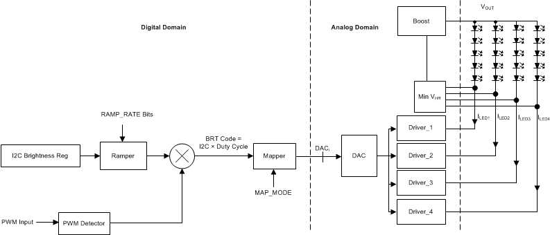
LM36274 LM36274_PWM_BRT_NORAMP.gifFigure 35. (I2C + PWM) Brightness Control, PWM Ramper Disabled
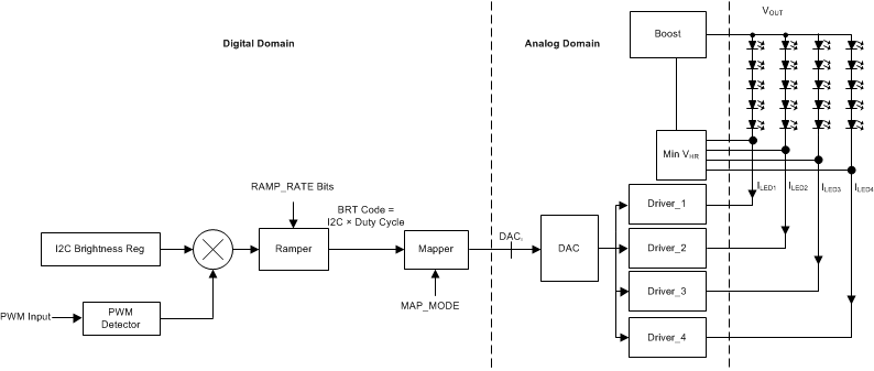
LM36274 LM36274_PWM_BRT.gifFigure 36. (I2C + PWM) Brightness Control, PWM Ramper Enabled