SNOS935C February 2001 – December 2014 LM321
PRODUCTION DATA.
- 1 Features
- 2 Applications
- 3 Description
- 4 Revision History
- 5 Pin Configuration and Functions
- 6 Specifications
- 7 Detailed Description
- 8 Application and Implementation
- 9 Power Supply Recommendations
- 10Layout
- 11Device and Documentation Support
- 12Mechanical, Packaging, and Orderable Information
5 Pin Configuration and Functions
DBV Package
5-Pin SOT-23
Top View
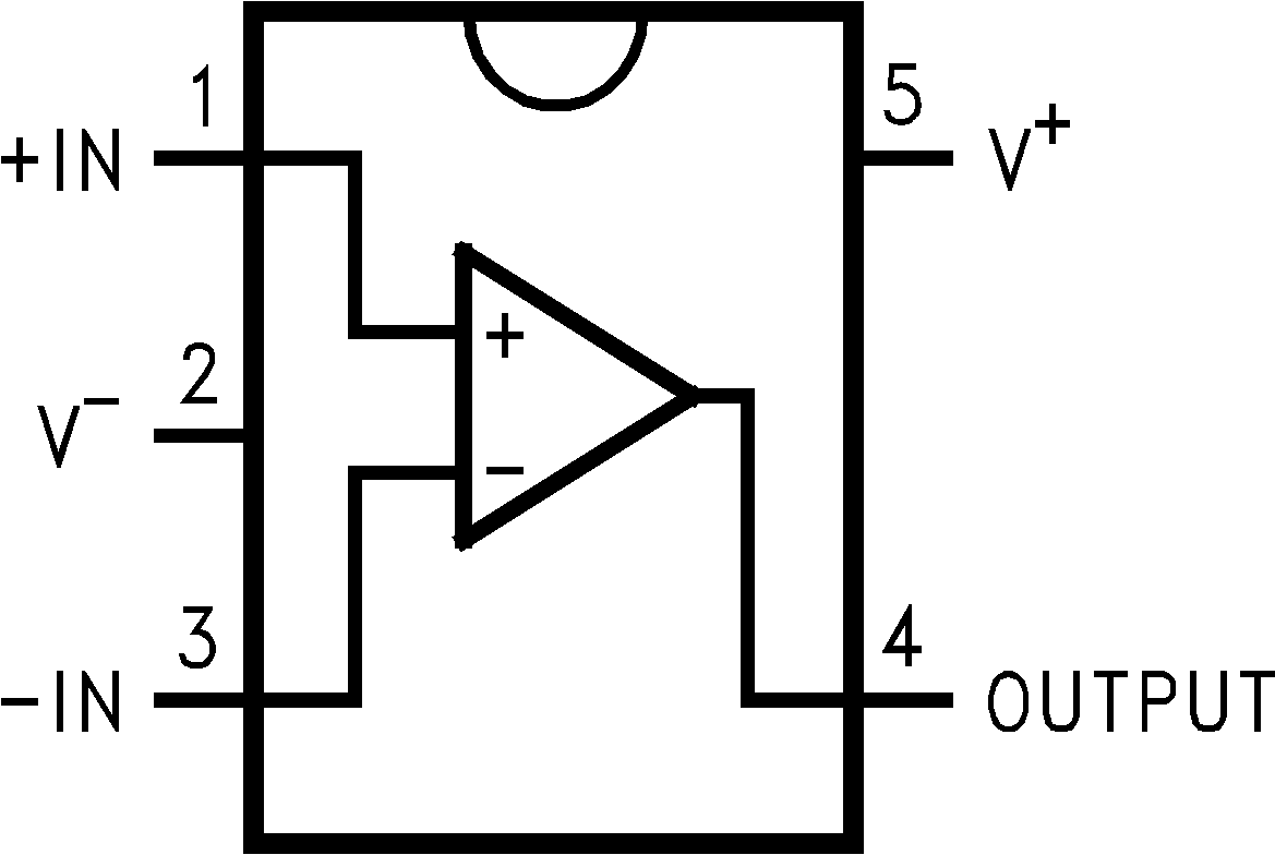
Pin Functions
| PIN | I/O | DESCRIPTION | |
|---|---|---|---|
| NAME | NO. | ||
| +IN | 1 | I | Noninverting input |
| V– | 2 | — | Negative (lowest) power supply |
| –IN | 3 | I | Inverting input |
| OUTPUT | 4 | O | Output |
| V+ | 5 | — | Positive (highest) power supply |