ZHCSBF2B August 2013 – November 2014 LM27403
PRODUCTION DATA.
- 1 特性
- 2 应用范围
- 3 说明
- 4 修订历史记录
- 5 说明 (续)
- 6 Pin Configuration and Functions
- 7 Specifications
-
8 Detailed Description
- 8.1 Overview
- 8.2 Functional Block Diagram
- 8.3
Feature Description
- 8.3.1 Input Range: VIN
- 8.3.2 Output Voltage: FB Voltage and Accuracy
- 8.3.3 Input and Bias Rail Voltages: VIN and VDD
- 8.3.4 Precision Enable: UVLO/EN
- 8.3.5 Switching Frequency
- 8.3.6 Temperature Sensing: D+ and D-
- 8.3.7 Thermal Shutdown: OTP
- 8.3.8 Inductor-DCR-Based Overcurrent Protection
- 8.3.9 Current Sensing: CS+ and CS-
- 8.3.10 Current Limit Handling
- 8.3.11 Soft-Start: SS/TRACK
- 8.3.12 Monotonic Startup
- 8.3.13 Prebias Startup
- 8.3.14 Voltage-Mode Control
- 8.3.15 Output Voltage Remote Sense: RS
- 8.3.16 Power Good: PGOOD
- 8.3.17 Gate Drivers: LG and HG
- 8.3.18 Sink and Source Capability
- 8.4 Device Functional Modes
-
9 Application and Implementation
- 9.1 Application Information
- 9.2
Typical Applications
- 9.2.1 Design 1 - High-Efficiency Synchronous Buck Regulator for Telecom Power
- 9.2.2 Design 2 - Powering FPGAs Using Flexible 30A Regulator With Small Footprint
- 9.2.3 Design 3 - Powering Multicore DSPs
- 9.2.4 Design 4 - Regulated 12-V Rail with LDO Low-Noise Auxiliary Output for RF Power
- 9.2.5 Design 5 - High Power Density Implementation From 3.3-V or 5-V Supply Rail
- 10Power Supply Recommendations
- 11Layout
- 12器件和文档支持
- 13机械、封装和可订购信息
7 Specifications
7.1 Absolute Maximum Ratings
over operating free-air temperature range (unless otherwise noted)(1).| MIN | MAX | UNIT | ||
|---|---|---|---|---|
| Voltage(2) | VIN, CS+, CS–, SW(3)(5) | –0.3 | 22 | V |
| VDD, PGOOD | –0.3 | 6 | V | |
| SS/TRACK, SYNC, FADJ, COMP, FB, RS | –0.3 | VVDD + 0.3 | V | |
| UVLO/EN | –0.3 | min (VVIN + 0.3, 6) | V | |
| CBOOT(4) | –0.3 | 24 | V | |
| CBOOT to SW | –0.3 | 6 | V | |
| CS+ to CS– | –1 | 1 | V | |
| OTP, D+, D– | –0.3 | VVDD | V | |
| Thermal | Operating junction temperature, TJ | –40 | 150 | °C |
(1) Stresses beyond those listed under Absolute Maximum Ratings may cause permanent damage to the device. These are stress ratings only and functional operation of the device at these or any other condition beyond those included under Recommended Operating Conditions is not implied. Exposure to absolute-maximum-rated conditions for extended periods of time may affect device reliability.
(2) All voltages are with respect to the network ground pin unless otherwise noted.
(3) The SW pin can tolerate negative voltage spikes as low as –10 V and as high as 30 V for a duration up to 10 ns.
(4) The CBOOT pin can tolerate positive voltage spikes as high as 35 V for a duration up to 10 ns.
(5) Body diode of the low-side MOSFET notwithstanding, parasitic inductance in a real application may result in the SW voltage ringing negative.
7.2 Handling Ratings
| MIN | MAX | UNIT | |||
|---|---|---|---|---|---|
| Tstg | Storage temperature range | –65 | 150 | °C | |
| V(ESD) | Electrostatic discharge | Human body model (HBM), per ANSI/ESDA/JEDEC JS-001, all pins(1) | –2 | 2 | kV |
| Charged device model (CDM), per JEDEC specification JESD22-C101, all pins(2) | –500 | 500 | V | ||
(1) JEDEC document JEP155 states that 500-V HBM allows safe manufacturing with a standard ESD control process.
(2) JEDEC document JEP157 states that 250-V CDM allows safe manufacturing with a standard ESD control process.
7.3 Recommended Operating Conditions
over operating free-air temperature range (unless otherwise noted)(1).| MIN | NOM | MAX | UNIT | |||
|---|---|---|---|---|---|---|
| VIN | Input voltage(2) | VIN tied to VDD | 3.0 | 5.5 | V | |
| VIN | 3.0 | 20 | V | |||
| SW | SW pin voltage | –0.3 | 20 | V | ||
| VDD | VDD pin voltage | 2.6 | 4.7 | 5.5 | V | |
| PGOOD | PGOOD pin voltage | 0 | 5.5 | V | ||
| UVLO/EN | UVLO/EN pin voltage | 0 | min (VVIN, 5.5) | V | ||
| SS/TRACK | SS/TRACK pin voltage | 0 | VVDD | V | ||
| SYNC | SYNC pin voltage | 0 | 5.5 | V | ||
| RS | RS pin voltage | –0.1 | 0.1 | V | ||
| TJ | Operating junction temperature | –40 | +125 | °C | ||
| TA | Operating free-air temperature | –40 | +125 | °C | ||
(1) Recommended Operating Conditions are conditions under which operation of the device is intended to be functional but does not guarantee performance limits.
(2) VDD is the output of the internal linear regulator bias supply. Under normal operating conditions, where VIN is greater than 5.5 V, VDD must not be tied to any external voltage source. In an application where VIN is between 3.0 V and 5.5 V, connecting VIN to VDD maximizes the bias supply rail voltage.
7.4 Thermal Information
| THERMAL METRIC(1) | LM27403 | UNIT | |
|---|---|---|---|
| RTW | |||
| 24 PINS | |||
| θJA | Junction-to-ambient thermal resistance | 32.7 | °C/W |
| θJCtop | Junction-to-case (top) thermal resistance | 31.2 | |
| θJB | Junction-to-board thermal resistance | 11.2 | |
| ψJT | Junction-to-top characterization parameter | 0.2 | |
| ψJB | Junction-to-board characterization parameter | 11.2 | |
| θJCbot | Junction-to-case (bottom) thermal resistance | 1.4 | |
(1) For more information about traditional and new thermal metrics, see the IC Package Thermal Metrics application report, SPRA953.
7.5 Electrical Characteristics
Typical values correspond to TJ = 25°C. Minimum and maximum limits apply over –40°C to +125°C junction temperature range unless otherwise stated(1),(2). VVIN = 12 V and all parameters at zero power dissipation (unless otherwise noted).| PARAMETER | TEST CONDITIONS | MIN | TYP | MAX | UNIT | ||
|---|---|---|---|---|---|---|---|
| OPERATIONAL SPECIFICATIONS | |||||||
| IQ | Quiescent current | VFB = 0.6 V (not switching) | 3.5 | 5.0 | mA | ||
| IQ-SD | Shutdown quiescent current | VUVLO/EN = 0 V | 25 | 45 | µA | ||
| REFERENCE | |||||||
| VFB | FB pin voltage accuracy | 594 | 600 | 606 | mV | ||
| IFB | FB pin bias current | VFB = 0.65 V | –165 | 0 | 165 | nA | |
| INTERNAL UVLO | |||||||
| UVLO | Input undervoltage lockout | VVIN rising, VVDD rising | 2.6 | 2.7 | 2.8 | V | |
| UVLO_hys | UVLO hysteresis | VVIN falling, VVDD falling | 250 | mV | |||
| SWITCHING | |||||||
| FSW | Switching frequency | RFADJ = 4.12 kΩ | 925 | 1050 | 1150 | kHz | |
| RFADJ = 20 kΩ | 435 | 500 | 555 | kHz | |||
| RFADJ = 95.3 kΩ | 185 | 215 | 250 | kHz | |||
| DMAX | Maximum duty cycle | FSW = 500 kHz | 90% | 93% | |||
| TOFF-MIN | Minimum off-time | VFB = 0.5 V, FSW = 500 kHz | 110 | 150 | 190 | ns | |
| TON-MIN | Minimum controllable on-time | VFB = 0.7 V, FSW = 500 kHz | 30 | ns | |||
| VDD SUBREGULATOR AND BOOT | |||||||
| VDD | Subregulator output voltage | IVDD = 25 mA | 4.2 | 4.7 | 5.3 | V | |
| VDDVDO | Dropout voltage | IVDD = 15 mA, VVIN = 3.0 V | 150 | mV | |||
| VDDCL | VDD current limit | VVDD = 4.0 V | 106 | mA | |||
| IQBOOT | CBOOT pin leakage current | VCBOOT – VSW = 4.5 V | 0.5 | nA | |||
| ERROR AMPLIFIER | |||||||
| BW-3dB | Error amplifier open-loop bandwidth | 6 | MHz | ||||
| AVOL | Error amplifier dc gain | 70 | dB | ||||
| ISOURCE | COMP source current | VFB = 0.5 V | 1 | mA | |||
| ISINK | COMP sink current | VFB = 0.7 V | 100 | µA | |||
| VCOMP-MAX | Maximum COMP voltage | VFB = 0.5 V | 3.9 | V | |||
| VCOMP-MIN | Minimum COMP voltage | VFB = 0.7 V | 0.5 | V | |||
| OVERCURRENT PROTECTION | |||||||
| VCS_OFFSET | Current limit comparator offset voltage | –3.5 | 0 | 3.5 | mV | ||
| ICS | Current limit offset current | VCS– = 3 V, ΔVBE = 59.4 mV(3), TJ = 25°C | 9.3 | 9.9 | 10.5 | µA | |
| VCS– = 3 V, D+ shorted to D– | 3.4 | 5.0 | 6.6 | µA | |||
| ICS-CV1 | ICS compliance voltage | VVIN – VCS–, ΔICS < 5% | VVIN = 12 V | 800 | mV | ||
| ICS-CV2 | VVIN = 3 V | 800 | mV | ||||
| ICS-TC | ICS temperature coefficient | Referenced to ΔVBE(5) | 160 | 187 | 212 | nA/mV | |
| TCL-DELAY | Current limit hiccup delay | 5 | ms | ||||
| GATE DRIVERS | |||||||
| RDS(ON)1 | High-side MOSFET driver on-state resistance | VCBOOT – VSW = 4.5 V | IHG = 0.1 A (pullup) | 1.5 | Ω | ||
| RDS(ON)2 | IHG = –0.1 A (pulldown) | 1.0 | Ω | ||||
| IDRV-HG-SRC | High-side MOSFET driver peak current | CLOAD = 3 nF | Source current (pullup) | 1.5 | A | ||
| IDRV-HG-SINK | Sink current (pulldown) | 2.0 | A | ||||
| RDS(ON)3 | Low-side MOSFET driver on-state resistance | VDD = 4.5 V | ILG = 0.1 A (pullup) | 1.5 | Ω | ||
| RDS(ON)4 | ILG = –0.1 A (pulldown) | 0.9 | Ω | ||||
| IDRV-LG-SRC | Low-side MOSFET driver peak current | CLOAD = 3 nF | Source current (pullup) | 1.5 | A | ||
| IDRV-LG-SINK | Sink current (pulldown) | 2.0 | A | ||||
| TDEAD | Adaptive dead-time | 15 | ns | ||||
| SOFT-START | |||||||
| ISS | Soft-start source current | VSS/TRACK = 0 V | 1.0 | 3.0 | 5.0 | µA | |
| ISS-PD | Soft-start pulldown resistance | VSS/TRACK = 0.6 V | 330 | Ω | |||
| TSS-INT | Internal soft-start timeout | 1.28 | ms | ||||
| POWER GOOD | |||||||
| IPGS | PGOOD low sink current | VPGOOD = 0.2 V, VFB = 0.75 V | 70 | 100 | µA | ||
| IPGL | PGOOD leakage current | VPGOOD = 5 V | 1 | 10 | µA | ||
| OVT | Overvoltage threshold | VFB rising, RS tied to GND | 111% | 116.5% | 123% | ||
| OVTHYS | OVT hysteresis | VFB falling, RS tied to GND | 3.5% | ||||
| UVT | Undervoltage threshold | VFB rising, RS tied to GND | 86% | 91% | 97% | ||
| UVTHYS | UVT hysteresis | VFB falling, RS tied to GND | 4% | ||||
| tdeglitch | Deglitch time | VPGOOD rising and falling | 20 | µs | |||
| UVLO/ENABLE | |||||||
| VUVLO1 | Logic low threshold | VUVLO/EN falling | 0.94 | 0.985 | 1.03 | V | |
| VUVLO2 | Logic high threshold | VUVLO/EN rising | 1.11 | 1.15 | 1.18 | V | |
| VUVLO-HYS | UVLO/EN voltage hysteresis | VUVLO/EN falling | 139 | 165 | 190 | mV | |
| IUVLO1 | UVLO/EN pullup current, disabled | VUVLO/EN = 0 V | 0.8 | 1.8 | 2.7 | µA | |
| IUVLO2 | UVLO/EN pullup current, enabled | VUVLO/EN = 1.25 V | 5.5 | 10.5 | 15.5 | µA | |
| CLOCK SYNCHRONIZATION | |||||||
| VIH-SYNC | SYNC pin VIH | 2 | V | ||||
| VIL-SYNC | SYNC pin VIL | 0.8 | V | ||||
| SYNCFSW-L | Minimum clock sync frequency | 200 | kHz | ||||
| SYNCFSW-H | Maximum clock sync frequency | 1.2 | MHz | ||||
| SYNCI | SYNC pin input current | 1 | µA | ||||
| EXTERNAL TEMPERATURE SENSE AND THERMAL SHUTDOWN | |||||||
| ID+1 | D+ pin state 1 current | 10 | µA | ||||
| ID+2 | D+ pin state 2 current | 100 | µA | ||||
| IOTP | Remote thermal current | ΔVBE = 79.3 mV(4) | 13.5 | 14.6 | 15.5 | µA | |
| IOTP-TC | IOTP temperature coefficient | Referenced to ΔVBE(5) | 158 | 187 | 213 | nA/mV | |
| VTRIP | Remote thermal trip point | 1.15 | V | ||||
| VTRIP-HYS | Remote thermal trip point hysteresis | 80 | mV | ||||
| ROTP | OTP resistance, thermal shutdown | ROTP(nom) = 80.7 kΩ, ΔVBE = 79.3 mV(4), TJ = 125°C | –5% | 5% | |||
| TSHD | Internal thermal shutdown threshold | Rising | 150 | °C | |||
| TSHD-HYS | Internal thermal shutdown threshold hysteresis | 20 | °C | ||||
(1) All hot and cold limits are specified by correlating the electrical characteristic to process and temperature variations and applying statistical process control.
(2) The junction temperature (TJ in °C) is calculated from the ambient temperature (TA in °C) and power dissipation (PD in Watts) as follows: TJ = TA + (PD × θJA) where (°C/W) is the package thermal impedance provided in the Thermal Information section.
(3) The specified parameter is calculated based on a 2N3904 transistor at 25°C.
(4) The specified parameter is calculated based on a 2N3904 transistor at 125°C.
(5) Multiply by 19.9 to scale from nA/mV to ppm/°C (assumes 2N3904 BJT temperature sensor with ideality factor η =1.004).
7.6 Typical Characteristics
Unless otherwise stated, all datasheet curves were recorded using the circuit and powertrain designated in Figure 41 with input and output voltages of 12 V and 1.2 V, respectively, and switching frequency of 250 kHz.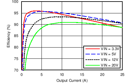 Figure 1. Efficiency Plot, VOUT = 1.2 V
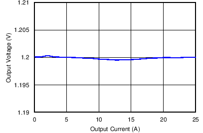 Figure 3. Load Regulation
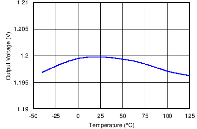 Figure 5. Temperature Regulation
 Figure 7. Shutdown Quiescent Current vs. Temperature
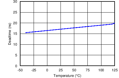 Figure 9. Deadtime vs. Temperature
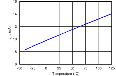 Figure 11. OTP Current vs. Temperature
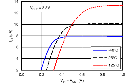 Figure 13. CS– Current Source Compliance Voltage
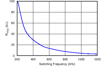 Figure 15. Switching Frequency vs. Frequency Adjust Resistance
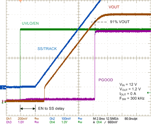 Figure 17. Start-up Characteristic
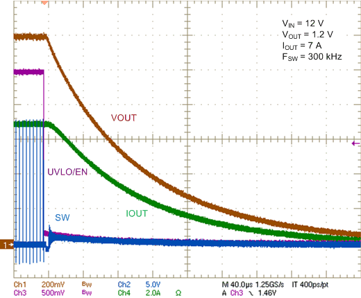 Figure 19. Shutdown Characteristic
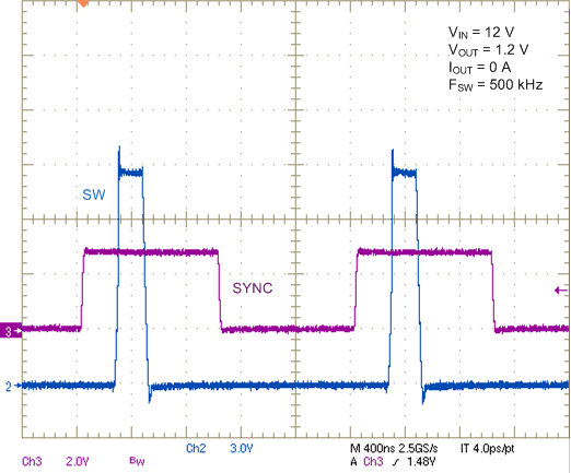 Figure 21. SYNC Waveform
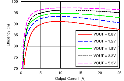 Figure 2. Efficiency Plot, VIN = 12 V
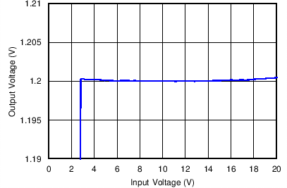 Figure 4. Line Regulation
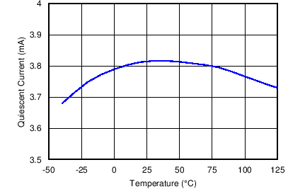 Figure 6. Quiescent Current vs. Temperature, Nonswitching
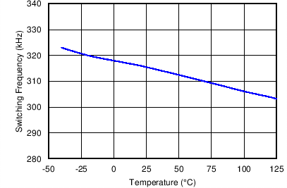 Figure 8. Switching Frequency vs. Temperature
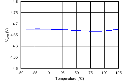 Figure 10. VDD Voltage vs. Temperature
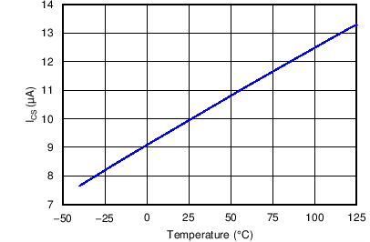 Figure 12. CS– Current vs. Temperature
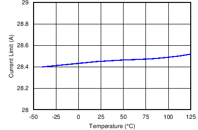 Figure 14. Current Limit Inception vs. Temperature
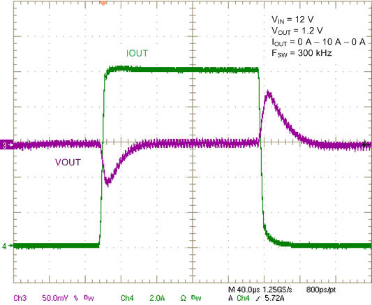 Figure 16. 10-A Step Load Transient Response, 2.5-A/µs Slew Rate
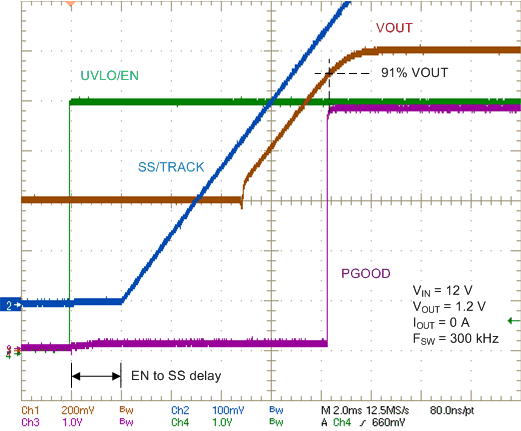 Figure 18. Prebias Start-up Characteristic
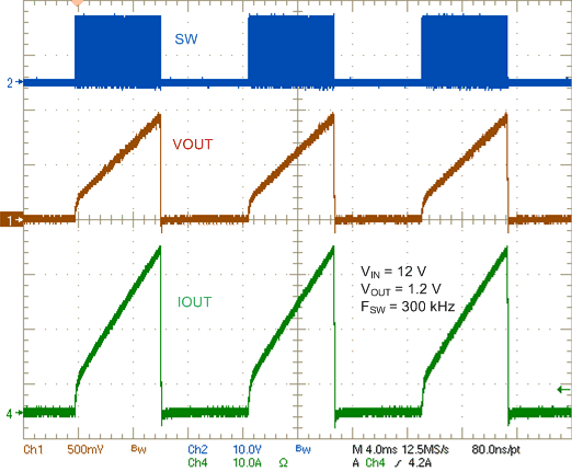 Figure 20. Current Limit Hiccup Mode
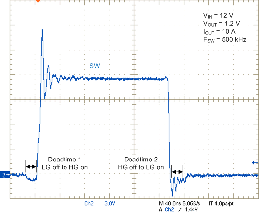 Figure 22. Switch Node Waveform