SNVS487E December 2006 – January 2015 LM27313 , LM27313-Q1
PRODUCTION DATA.
- 1 Features
- 2 Applications
- 3 Description
- 4 Revision History
- 5 Pin Configuration and Functions
- 6 Specifications
- 7 Detailed Description
-
8 Application and Implementation
- 8.1 Application Information
- 8.2
Typical Applications
- 8.2.1
Application Circuit VIN=5.0 V, VOUT=12.0 V, Iload=250 mA
- 8.2.1.1 Design Requirements
- 8.2.1.2
Detailed Design Procedure
- 8.2.1.2.1 Selecting the External Capacitors
- 8.2.1.2.2 Selecting the Output Capacitor
- 8.2.1.2.3 Selecting the Input Capacitor
- 8.2.1.2.4 Feed-Forward Compensation
- 8.2.1.2.5 Selecting Diodes
- 8.2.1.2.6 Setting the Output Voltage
- 8.2.1.2.7 Duty Cycle
- 8.2.1.2.8 Inductance Value
- 8.2.1.2.9 Maximum Switch Current
- 8.2.1.2.10 Calculating Load Current
- 8.2.1.2.11 Design Parameters VSW and ISW
- 8.2.1.2.12 Minimum Inductance
- 8.2.1.2.13 Inductor Suppliers
- 8.2.1.2.14 Shutdown Pin Operation
- 8.2.1.3 Application Curves
- 8.2.2 Application Circuit VIN=5.0V, VOUT=20.0V, Iload=150mA
- 8.2.1
Application Circuit VIN=5.0 V, VOUT=12.0 V, Iload=250 mA
- 9 Power Supply Recommendations
- 10Layout
- 11Device and Documentation Support
- 12Mechanical, Packaging, and Orderable Information
10 Layout
10.1 Layout Guidelines
High-frequency switching regulators require very careful layout of components in order to get stable operation and low noise. All components must be as close as possible to the LM27313 device. It is recommended that a 4-layer PCB be used so that internal ground planes are available.
Some additional guidelines to be observed:
- Keep the path between L1, D1, and C2 extremely short. Parasitic trace inductance in series with D1 and C2 will increase noise and ringing.
- The feedback components R1, R2 and CF must be kept close to the FB pin of the LM27313 to prevent noise injection on the high impedance FB pin.
- If internal ground planes are available (recommended) use vias to connect directly to the LM27313 ground at device pin 2, as well as the negative sides of capacitors C1 and C2.
10.2 Layout Example
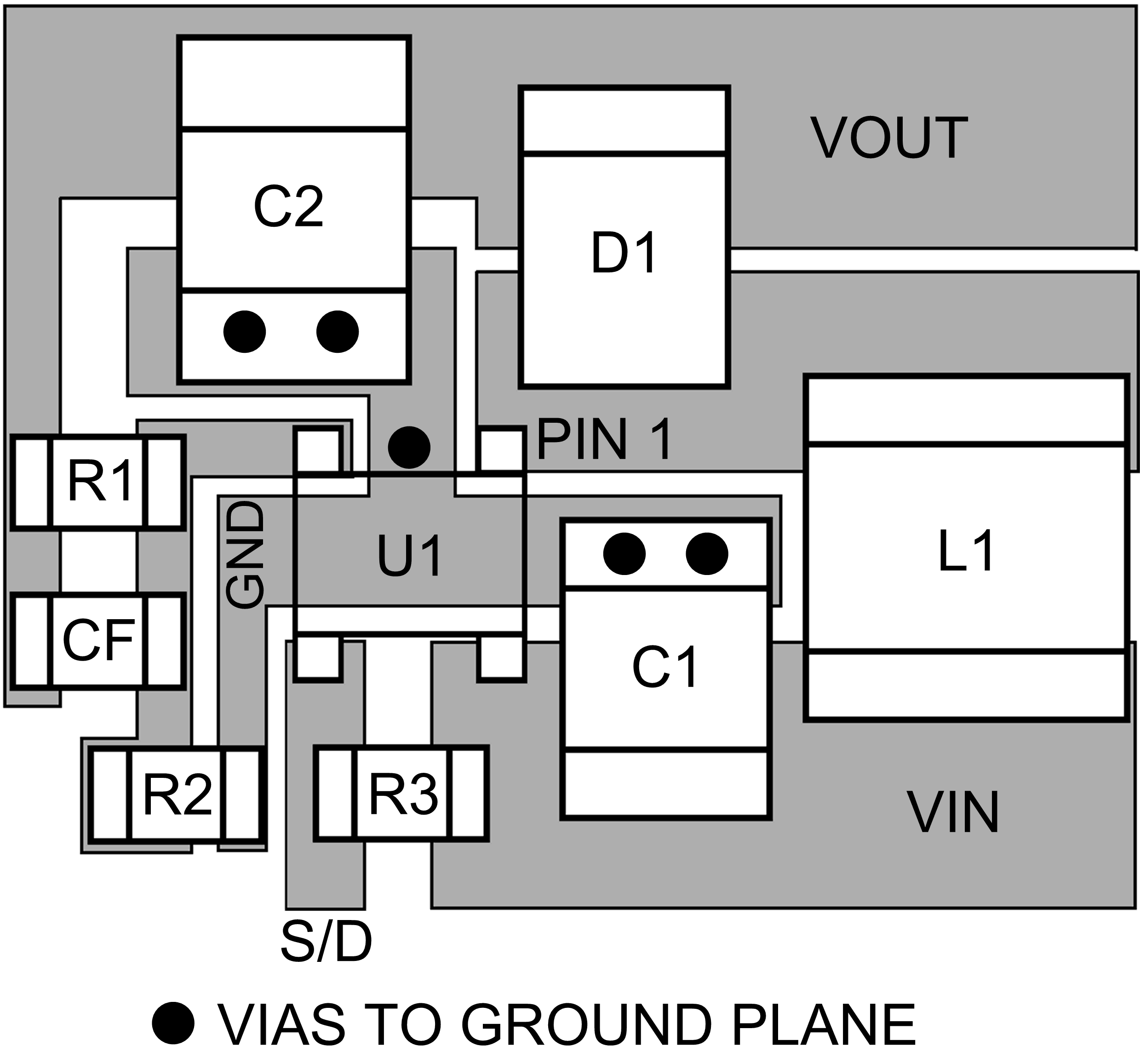 Figure 22. Recommended PCB Component Layout
10.3 Thermal Considerations
At higher duty cycles, the increased ON time of the FET means the maximum output current will be determined by power dissipation within the LM27313 FET switch. The switch power dissipation from ON-state conduction is calculated by:
There will be some switching losses as well, so some derating needs to be applied when calculating IC power dissipation.