SNIS144G July 2007 – September 2016 LM26LV , LM26LV-Q1
PRODUCTION DATA.
- 1 Features
- 2 Applications
- 3 Description
- 4 Revision History
- 5 Pin Configuration and Functions
- 6 Specifications
-
7 Detailed Description
- 7.1 Overview
- 7.2 Functional Block Diagram
- 7.3 Feature Description
- 7.4 Device Functional Modes
- 8 Application and Implementation
- 9 Power Supply Recommendations
- 10Layout
- 11Device and Documentation Support
- 12Mechanical, Packaging, and Orderable Information
7 Detailed Description
7.1 Overview
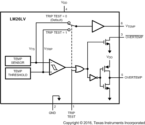
The LM26LV and LM26LV-Q1 are precision, dual-output, temperature switches with analog temperature sensor output. The trip temperature (TTRIP) is factory selected by the order number. The VTEMP class AB analog output provides a voltage that is proportional to temperature. The LM26LV and LM26LV-Q1 include an internal reference DAC (TEMP THRESHOLD), analog temperature sensor and analog comparator. The reference DAC is connected to one of the comparator inputs. The reference DAC output voltage (VTRIP) is preprogrammed by TI. The result of the reference DAC voltage and the temperature sensor output comparison is provided on two output pins OVERTEMP and OVERTEMP.
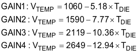
The VTEMP output has a programmable gain. The output gain has 4 possible settings as described in Table 1. The gain setting is dependent on the temperature trip point selected.
Built-in temperature hysteresis (THYST) prevents the digital outputs from oscillating. The OVERTEMP and OVERTEMP activates when the die temperature exceeds TTRIP and releases when the temperature falls below a temperature equal to TTRIP minus THYST. OVERTEMP is active-high with a push-pull structure. OVERTEMP, is active-low with an open-drain structure. The comparator hysteresis is fixed at 5°C.
Driving the TRIP-TEST high activates the digital outputs. A processor can check the logic level of the OVERTEMP or OVERTEMP, confirming that they changed to their active state. This allows for system production testing verification that the comparator and output circuitry are functional after system assembly. When the TRIP-TEST pin is high, the trip-level reference voltage appears at the VTEMP pin. Tying OVERTEMP to TRIP-TEST latches the output after it trips. It can be cleared by forcing TRIP-TEST low or powering off the LM26LV or LM26LV-Q1.
7.2 Functional Block Diagram
7.3 Feature Description
7.3.1 LM26LV and LM26LV-Q1 VTEMP vs Die Temperature Conversion Table
The LM26LV and LM26LV-Q1 have one out of four possible factory-set gains, Gain 1 through Gain 4, depending on the range of the Temperature Trip Point. The VTEMP temperature sensor voltage, in millivolts, at each discrete die temperature over the complete operating temperature range, and for each of the four Temperature Trip Point ranges, is shown in Table 1. This table is the reference from which the LM26LV and LM26LV-Q1 accuracy specifications (listed in Accuracy Characteristics) are determined. This table can be used, for example, in a host processor look-up table. See The Second-Order Equation (Parabolic) for the parabolic equation used in the Conversion Table.
Table 1. VTEMP Temperature Sensor Output Voltage vs Die Temperature Conversion Table
| DIE TEMPERATURE (°C) | ANALOG OUTPUT VOLTAGE, VTEMP (mV)(1) | |||
|---|---|---|---|---|
| GAIN 1 | GAIN 2 | GAIN 3 | GAIN 4 | |
| –50 | 1312 | 1967 | 2623 | 3278 |
| –49 | 1307 | 1960 | 2613 | 3266 |
| –48 | 1302 | 1952 | 2603 | 3253 |
| –47 | 1297 | 1945 | 2593 | 3241 |
| –46 | 1292 | 1937 | 2583 | 3229 |
| –45 | 1287 | 1930 | 2573 | 3216 |
| –44 | 1282 | 1922 | 2563 | 3204 |
| –43 | 1277 | 1915 | 2553 | 3191 |
| –42 | 1272 | 1908 | 2543 | 3179 |
| –41 | 1267 | 1900 | 2533 | 3166 |
| –40 | 1262 | 1893 | 2523 | 3154 |
| –39 | 1257 | 1885 | 2513 | 3141 |
| –38 | 1252 | 1878 | 2503 | 3129 |
| –37 | 1247 | 1870 | 2493 | 3116 |
| –36 | 1242 | 1863 | 2483 | 3104 |
| –35 | 1237 | 1855 | 2473 | 3091 |
| –34 | 1232 | 1848 | 2463 | 3079 |
| –33 | 1227 | 1840 | 2453 | 3066 |
| –32 | 1222 | 1833 | 2443 | 3054 |
| –31 | 1217 | 1825 | 2433 | 3041 |
| –30 | 1212 | 1818 | 2423 | 3029 |
| –29 | 1207 | 1810 | 2413 | 3016 |
| –28 | 1202 | 1803 | 2403 | 3004 |
| –27 | 1197 | 1795 | 2393 | 2991 |
| –26 | 1192 | 1788 | 2383 | 2979 |
| –25 | 1187 | 1780 | 2373 | 2966 |
| –24 | 1182 | 1773 | 2363 | 2954 |
| –23 | 1177 | 1765 | 2353 | 2941 |
| –22 | 1172 | 1757 | 2343 | 2929 |
| –21 | 1167 | 1750 | 2333 | 2916 |
| –20 | 1162 | 1742 | 2323 | 2903 |
| –19 | 1157 | 1735 | 2313 | 2891 |
| –18 | 1152 | 1727 | 2303 | 2878 |
| –17 | 1147 | 1720 | 2293 | 2866 |
| –16 | 1142 | 1712 | 2283 | 2853 |
| –15 | 1137 | 1705 | 2272 | 2841 |
| –14 | 1132 | 1697 | 2262 | 2828 |
| –13 | 1127 | 1690 | 2252 | 2815 |
| –12 | 1122 | 1682 | 2242 | 2803 |
| –11 | 1116 | 1674 | 2232 | 2790 |
| –10 | 1111 | 1667 | 2222 | 2777 |
| –9 | 1106 | 1659 | 2212 | 2765 |
| –8 | 1101 | 1652 | 2202 | 2752 |
| –7 | 1096 | 1644 | 2192 | 2740 |
| –6 | 1091 | 1637 | 2182 | 2727 |
| –5 | 1086 | 1629 | 2171 | 2714 |
| –4 | 1081 | 1621 | 2161 | 2702 |
| –3 | 1076 | 1614 | 2151 | 2689 |
| –2 | 1071 | 1606 | 2141 | 2676 |
| –1 | 1066 | 1599 | 2131 | 2664 |
| 0 | 1061 | 1591 | 2121 | 2651 |
| 1 | 1056 | 1583 | 2111 | 2638 |
| 2 | 1051 | 1576 | 2101 | 2626 |
| 3 | 1046 | 1568 | 2090 | 2613 |
| 4 | 1041 | 1561 | 2080 | 2600 |
| 5 | 1035 | 1553 | 2070 | 2587 |
| 6 | 1030 | 1545 | 2060 | 2575 |
| 7 | 1025 | 1538 | 2050 | 2562 |
| 8 | 1020 | 1530 | 2040 | 2549 |
| 9 | 1015 | 1522 | 2029 | 2537 |
| 10 | 1010 | 1515 | 2019 | 2524 |
| 11 | 1005 | 1507 | 2009 | 2511 |
| 12 | 1000 | 1499 | 1999 | 2498 |
| 13 | 995 | 1492 | 1989 | 2486 |
| 14 | 990 | 1484 | 1978 | 2473 |
| 15 | 985 | 1477 | 1968 | 2460 |
| 16 | 980 | 1469 | 1958 | 2447 |
| 17 | 974 | 1461 | 1948 | 2435 |
| 18 | 969 | 1454 | 1938 | 2422 |
| 19 | 964 | 1446 | 1927 | 2409 |
| 20 | 959 | 1438 | 1917 | 2396 |
| 21 | 954 | 1431 | 1907 | 2383 |
| 22 | 949 | 1423 | 1897 | 2371 |
| 23 | 944 | 1415 | 1886 | 2358 |
| 24 | 939 | 1407 | 1876 | 2345 |
| 25 | 934 | 1400 | 1866 | 2332 |
| 26 | 928 | 1392 | 1856 | 2319 |
| 27 | 923 | 1384 | 1845 | 2307 |
| 28 | 918 | 1377 | 1835 | 2294 |
| 29 | 913 | 1369 | 1825 | 2281 |
| 30 | 908 | 1361 | 1815 | 2268 |
| 31 | 903 | 1354 | 1804 | 2255 |
| 32 | 898 | 1346 | 1794 | 2242 |
| 33 | 892 | 1338 | 1784 | 2230 |
| 34 | 887 | 1331 | 1774 | 2217 |
| 35 | 882 | 1323 | 1763 | 2204 |
| 36 | 877 | 1315 | 1753 | 2191 |
| 37 | 872 | 1307 | 1743 | 2178 |
| 38 | 867 | 1300 | 1732 | 2165 |
| 39 | 862 | 1292 | 1722 | 2152 |
| 40 | 856 | 1284 | 1712 | 2139 |
| 41 | 851 | 1276 | 1701 | 2127 |
| 42 | 846 | 1269 | 1691 | 2114 |
| 43 | 841 | 1261 | 1681 | 2101 |
| 44 | 836 | 1253 | 1670 | 2088 |
| 45 | 831 | 1245 | 1660 | 2075 |
| 46 | 825 | 1238 | 1650 | 2062 |
| 47 | 820 | 1230 | 1639 | 2049 |
| 48 | 815 | 1222 | 1629 | 2036 |
| 49 | 810 | 1214 | 1619 | 2023 |
| 50 | 805 | 1207 | 1608 | 2010 |
| 51 | 800 | 1199 | 1598 | 1997 |
| 52 | 794 | 1191 | 1588 | 1984 |
| 53 | 789 | 1183 | 1577 | 1971 |
| 54 | 784 | 1176 | 1567 | 1958 |
| 55 | 779 | 1168 | 1557 | 1946 |
| 56 | 774 | 1160 | 1546 | 1933 |
| 57 | 769 | 1152 | 1536 | 1920 |
| 58 | 763 | 1144 | 1525 | 1907 |
| 59 | 758 | 1137 | 1515 | 1894 |
| 60 | 753 | 1129 | 1505 | 1881 |
| 61 | 748 | 1121 | 1494 | 1868 |
| 62 | 743 | 1113 | 1484 | 1855 |
| 63 | 737 | 1105 | 1473 | 1842 |
| 64 | 732 | 1098 | 1463 | 1829 |
| 65 | 727 | 1090 | 1453 | 1816 |
| 66 | 722 | 1082 | 1442 | 1803 |
| 67 | 717 | 1074 | 1432 | 1790 |
| 68 | 711 | 1066 | 1421 | 1776 |
| 69 | 706 | 1059 | 1411 | 1763 |
| 70 | 701 | 1051 | 1400 | 1750 |
| 71 | 696 | 1043 | 1390 | 1737 |
| 72 | 690 | 1035 | 1380 | 1724 |
| 73 | 685 | 1027 | 1369 | 1711 |
| 74 | 680 | 1019 | 1359 | 1698 |
| 75 | 675 | 1012 | 1348 | 1685 |
| 76 | 670 | 1004 | 1338 | 1672 |
| 77 | 664 | 996 | 1327 | 1659 |
| 78 | 659 | 988 | 1317 | 1646 |
| 79 | 654 | 980 | 1306 | 1633 |
| 80 | 649 | 972 | 1296 | 1620 |
| 81 | 643 | 964 | 1285 | 1607 |
| 82 | 638 | 957 | 1275 | 1593 |
| 83 | 633 | 949 | 1264 | 1580 |
| 84 | 628 | 941 | 1254 | 1567 |
| 85 | 622 | 933 | 1243 | 1554 |
| 86 | 617 | 925 | 1233 | 1541 |
| 87 | 612 | 917 | 1222 | 1528 |
| 88 | 607 | 909 | 1212 | 1515 |
| 89 | 601 | 901 | 1201 | 1501 |
| 90 | 596 | 894 | 1191 | 1488 |
| 91 | 591 | 886 | 1180 | 1475 |
| 92 | 586 | 878 | 1170 | 1462 |
| 93 | 580 | 870 | 1159 | 1449 |
| 94 | 575 | 862 | 1149 | 1436 |
| 95 | 570 | 854 | 1138 | 1422 |
| 96 | 564 | 846 | 1128 | 1409 |
| 97 | 559 | 838 | 1117 | 1396 |
| 98 | 554 | 830 | 1106 | 1383 |
| 99 | 549 | 822 | 1096 | 1370 |
| 100 | 543 | 814 | 1085 | 1357 |
| 101 | 538 | 807 | 1075 | 1343 |
| 102 | 533 | 799 | 1064 | 1330 |
| 103 | 527 | 791 | 1054 | 1317 |
| 104 | 522 | 783 | 1043 | 1304 |
| 105 | 517 | 775 | 1032 | 1290 |
| 106 | 512 | 767 | 1022 | 1277 |
| 107 | 506 | 759 | 1011 | 1264 |
| 108 | 501 | 751 | 1001 | 1251 |
| 109 | 496 | 743 | 990 | 1237 |
| 110 | 490 | 735 | 979 | 1224 |
| 111 | 485 | 727 | 969 | 1211 |
| 112 | 480 | 719 | 958 | 1198 |
| 113 | 474 | 711 | 948 | 1184 |
| 114 | 469 | 703 | 937 | 1171 |
| 115 | 464 | 695 | 926 | 1158 |
| 116 | 459 | 687 | 916 | 1145 |
| 117 | 453 | 679 | 905 | 1131 |
| 118 | 448 | 671 | 894 | 1118 |
| 119 | 443 | 663 | 884 | 1105 |
| 120 | 437 | 655 | 873 | 1091 |
| 121 | 432 | 647 | 862 | 1078 |
| 122 | 427 | 639 | 852 | 1065 |
| 123 | 421 | 631 | 841 | 1051 |
| 124 | 416 | 623 | 831 | 1038 |
| 125 | 411 | 615 | 820 | 1025 |
| 126 | 405 | 607 | 809 | 1011 |
| 127 | 400 | 599 | 798 | 998 |
| 128 | 395 | 591 | 788 | 985 |
| 129 | 389 | 583 | 777 | 971 |
| 130 | 384 | 575 | 766 | 958 |
| 131 | 379 | 567 | 756 | 945 |
| 132 | 373 | 559 | 745 | 931 |
| 133 | 368 | 551 | 734 | 918 |
| 134 | 362 | 543 | 724 | 904 |
| 135 | 357 | 535 | 713 | 891 |
| 136 | 352 | 527 | 702 | 878 |
| 137 | 346 | 519 | 691 | 864 |
| 138 | 341 | 511 | 681 | 851 |
| 139 | 336 | 503 | 670 | 837 |
| 140 | 330 | 495 | 659 | 824 |
| 141 | 325 | 487 | 649 | 811 |
| 142 | 320 | 479 | 638 | 797 |
| 143 | 314 | 471 | 627 | 784 |
| 144 | 309 | 463 | 616 | 770 |
| 145 | 303 | 455 | 606 | 757 |
| 146 | 298 | 447 | 595 | 743 |
| 147 | 293 | 438 | 584 | 730 |
| 148 | 287 | 430 | 573 | 716 |
| 149 | 282 | 422 | 562 | 703 |
| 150 | 277 | 414 | 552 | 690 |
7.3.2 VTEMP vs Die Temperature Approximations
The LM26LV's and LM26LV-Q1's VTEMP analog temperature output is very linear. Table 1 and the equation in The Second-Order Equation (Parabolic) represent the most accurate typical performance of the VTEMP voltage output versus temperature.
7.3.2.1 The Second-Order Equation (Parabolic)
The data from Table 1, or Equation 1, when plotted, has an umbrella-shaped parabolic curve. VTEMP is in mV.

7.3.2.2 The First-Order Approximation (Linear)
For a quicker approximation, although less accurate than the second-order, over the full operating temperature range the linear formula below can be used. Using Equation 2, with the constant and slope in the following set of equations, the best-fit VTEMP versus die temperature performance can be calculated with an approximation error less than 18 mV. VTEMP is in mV.
7.3.2.3 First-Order Approximation (Linear) Over Small Temperature Range
For a linear approximation, a line can easily be calculated over the desired temperature range from Table 1 using the two-point equation:

where
- V is in mV
- T is in °C
- T1 and V1 are the coordinates of the lowest temperature
- T2 and V2 are the coordinates of the highest temperature
For example, to determine the equation of a line with GAIN4, with a temperature from 20°C to 50°C, proceed using Equation 4, Equation 5, and Equation 6:

Using this method of linear approximation, the transfer function can be approximated for one or more temperature ranges of interest.
7.3.3 OVERTEMP and OVERTEMP Digital Outputs
The OVERTEMP active high, push-pull output and the OVERTEMP active low, open-drain output both assert at the same time whenever the die temperature reaches the factory preset temperature trip point. They also assert simultaneously whenever the TRIP_TEST pin is set high. Both outputs deassert when the die temperature goes below the temperature trip point hysteresis. These two types of digital outputs enable the user the flexibility to choose the type of output that is most suitable for his design.
Either the OVERTEMP or the OVERTEMP digital output pins can be left open if not used.
7.3.3.1 OVERTEMP Open-Drain Digital Output
The OVERTEMP active low, open-drain digital output, if used, requires a pullup resistor between this pin and VDD. The following section shows how to determine the pullup resistor value.
7.3.3.1.1 Determining the Pullup Resistor Value
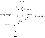
The pullup resistor value is calculated at the condition of maximum total current, IT, through the resistor. The total current is:
where
- IT is the maximum total current through the pullup resistor at VOL.
- IL is the load current, which is very low for typical digital inputs.
The pullup resistor maximum value can be found by using Equation 8.

where
- VDD(MAX) is the maximum power supply voltage to be used in the customer's system.
- VOUT is the Voltage at the OVERTEMP pin. Use VOL for calculating the pullup resistor.
7.3.3.1.1.1 Example Calculation
Suppose, for this example, a VDD of 3.3 V ± 0.3 V, a CMOS digital input as a load, a VOL of 0.2 V.
- For VOL of 0.2 V the electrical specification for OVERTEMP shows a maximum ISINK of 385 µA.
- Let IL = 1 µA, then IT is about 386 µA maximum. If 35 µA is selected as the current limit then IT for the calculation becomes 35 µA.
- VDD(MAX) is 3.3 V + 0.3 V = 3.6 V, then calculate the pullup resistor as RPULLUP = (3.6 – 0.2) / 35 µA = 97 kΩ.
- Based on this calculated value, select the closest resistor value in the tolerance family used.
In this example, if 5% resistor values are used, then the next closest value is 100 kΩ.
7.3.4 TRIP_TEST Digital Input
The TRIP_TEST pin simply provides a means to test the OVERTEMP and OVERTEMP digital outputs electronically by causing them to assert, at any operating temperature, as a result of forcing the TRIP_TEST pin high.
When the TRIP_TEST pin is pulled high the VTEMP pin is at the VTRIP voltage.
If not used, the TRIP_TEST pin may either be left open or grounded.
7.3.5 VTEMP Analog Temperature Sensor Output
The VTEMP push-pull output provides the ability to sink and source significant current. This is beneficial when, for example, driving dynamic loads like an input stage on an analog-to-digital converter (ADC). In these applications the source current is required to quickly charge the input capacitor of the ADC. See Application and Implementation for more discussion of this topic. The LM26LV and LM26LV-Q1 are ideal for applications which require strong source or sink current.
7.3.5.1 Noise Considerations
The LM26LV's and LM26LV-Q1's supply-noise rejection (the ratio of the AC signal on VTEMP to the AC signal on VDD) was measured during bench tests. The device's typical attenuation is shown in Typical Characteristics. A load capacitor on the output can help to filter noise.
For operation in very noisy environments, some bypass capacitance must be present on the supply within approximately 2 inches of the LM26LV or LM26LV-Q1.
7.3.5.2 Capacitive Loads
The VTEMP Output handles capacitive loading well. In an extremely noisy environment, or when driving a switched sampling input on an ADC, it may be necessary to add some filtering to minimize noise coupling. Without any precautions, the VTEMP can drive a capacitive load less than or equal to 1100 pF as shown in Figure 20. For capacitive loads greater than 1100 pF, a series resistor is required on the output, as shown in Figure 21, to maintain stable conditions.
 Figure 20. LM26LV or LM26LV-Q1 No Decoupling Required for Capacitive Loads Less Than 1100 pF.
 Figure 21. LM26LV or LM26LV-Q1 With Series Resistor for Capacitive Loading Greater Than 1100 pF
Table 2. Minimum Series Resistence for Capacitive Loads
| CLOAD | MINIMUM RS |
|---|---|
| 1.1 nF to 99 nF | 3 kΩ |
| 100 nF to 999 nF | 1.5 kΩ |
| 1 µF | 800 Ω |
7.3.5.3 Voltage Shift
The LM26LV and LM26LV-Q1 are very linear over temperature and supply voltage range. Due to the intrinsic behavior of an NMOS/PMOS rail-to-rail buffer, a slight shift in the output can occur when the supply voltage is ramped over the operating range of the device. The location of the shift is determined by the relative levels of VDD and VTEMP. The shift typically occurs when VDD – VTEMP = 1 V.
This slight shift (a few millivolts) takes place over a wide change (approximately 200 mV) in VDD or VTEMP. Because the shift takes place over a wide temperature change of 5°C to 20°C, VTEMP is always monotonic. The accuracy specifications Accuracy Characteristics already includes this possible shift.
7.4 Device Functional Modes
The LM26LV and LM26LV-Q1 have several modes of operation as detailed in the following drawings.
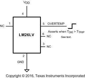 Figure 22. Temperature Switch Using Push-Pull Output
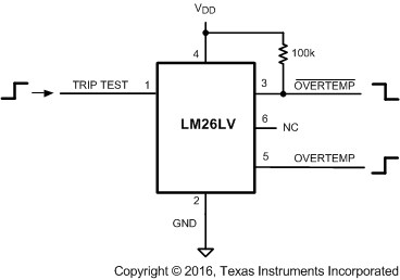 Figure 24. TRIP_TEST Digital Output Test Circuit
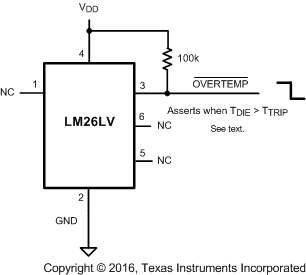 Figure 23. Temperature Switch Using Open-Drain Output
The TRIP_TEST pin, normally used to check the operation of the OVERTEMP and OVERTEMP pins, may be used to latch the outputs whenever the temperature exceeds the programmed limit and causes the digital outputs to assert. As shown in Figure 25, when OVERTEMP goes high the TRIP_TEST input is also pulled high and causes OVERTEMP output to latch high and the OVERTEMP output to latch low. The latch can be released by either momentarily pulling the TRIP_TEST pin low (GND), or by toggling the power supply to the device. The resistor limits the current out of the OVERTEMP output pin.
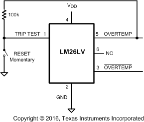 Figure 25. Latch Circuit Using OVERTEMP Output
Alternately, the circuit in Figure 25 the 100 kΩ can be replaced with a short and the momentary reset switch may be removed. In this configuration, when OVERTEMP goes active high, it drives TRIP_TEST high. THRIP TEST high causes OVERTEMP to stay high. It is therefore latched. To release the latch, power down, then power up the LM26LV or LM26LV-Q1. The LM26LV and LM26LV-Q1 always come up in a released condition.