ZHCSGW9 October 2017 LM2623-Q1
PRODUCTION DATA.
8 Applications and Implementation
NOTE
Information in the following applications sections is not part of the TI component specification, and TI does not warrant its accuracy or completeness. TI’s customers are responsible for determining suitability of components for their purposes. Customers should validate and test their design implementation to confirm system functionality.
8.1 Application Information
The LM2623-Q1 is suitable for automotive applications, and supports shutdown mode for low quiescent current when EN input is low. Output voltage level can be adjusted by changing feedback resistor divider values from 1.24-V to 14-V range. The maximum switching frequency is 2MHz.
8.2 Typical Application
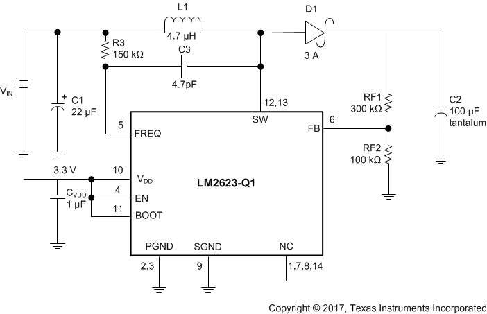
 Figure 9. LM2623-Q1 Typical Application
8.2.1 Design Requirements
The LM2623-Q1 allows the designer to vary output voltage, operating frequency and duty cycle to optimize device performance (see Detailed Design Procedure for details).
For typical boost-converter applications, use the parameters listed in Table 1.
Table 1. Design Parameters
| DESIGN PARAMETER | EXAMPLE VALUE |
|---|---|
| Input voltage | 0.9 V to 14 V |
| Output voltage | 1.24 V to 14 V (adjustable) |
| Output current | 2 A (maximum) |
8.2.2 Detailed Design Procedure
8.2.2.1 Non-Linear Effect
The LM2623-Q1 takes advantage of a non-linear effect, allowing for the duty cycle to be programmable. C3 in Figure 9 allows for the duty cycle to be programable.
8.2.2.2 Choosing the Correct C3 Capacitor
The duty cycle of the internal oscillator is programmable with the C3 capacitor. Choosing the correct C3 capacitor to obtain the appropriate duty cycle for a particular application circuit is a trial-and-error process. The non-linear effect that C3 produces is dependent on the input voltage and output voltage values. The correct C3 capacitor for specific input and output voltage values cannot be calculated. Choosing the correct C3 capacitance is best done by trial and error, in conjunction with the checking of the inductor peak current to make sure it is not too close to the current limit of the device. As the C3 capacitor value increases, so does the duty cycle; conversely, as the C3 capacitor value decreases, the duty cycle decreases. An incorrect choice of the C3 capacitor can result in the device prematurely tripping the current limit and/or double pulsing, which could lead to the output voltage not being stable. Optimizing the duty cycle for a given set of input/output voltages conditions can be done by referencing the component values in AN-1221 LM2623 General Purpose, Boost Converter Circuit.
8.2.2.3 Setting the Output Voltage
The output voltage of the step-up regulator can be set by connecting a feedback resistive divider made of RF1 and RF2. The resistor values are selected as follows:
A value of 50 kΩ to 100 kΩ is suggested for RF2. RF1 can be selected using Equation 1.
8.2.2.4 VDD Supply
The VDD supply must be between 3 V to 5 V for the LM2623-Q1 device. This voltage can be bootstrapped from a much lower input voltage by simply connecting the VDD pin to VOUT. In the event that the VDD supply voltage is not a low-ripple voltage source (less than 200 mV), it may be advisable to use an RC filter to clean it up. Excessive ripple on VDD may reduce the efficiency.
8.2.2.5 Setting the Switching Frequency
The switching frequency of the oscillator is selected by choosing an external resistor (R3) connected between VIN and the FREQ pin. See Figure 3 in the Typical Characteristics for choosing the R3 value to achieve the desired switching frequency. A high switching frequency allows the use of very small surface mount inductors and capacitors and results in a very small solution size. TI recommends a switching frequency between 300 kHz and 2 MHz.
8.2.2.6 Output Diode Selection
Use a Schottky diode for the output diode. The forward current rating of the diode must be higher than the peak input current, and the reverse voltage rating must be higher than the output voltage. Do not use ordinary rectifier diodes, because slow switching speeds and long recovery times cause the efficiency and the load regulation to suffer.
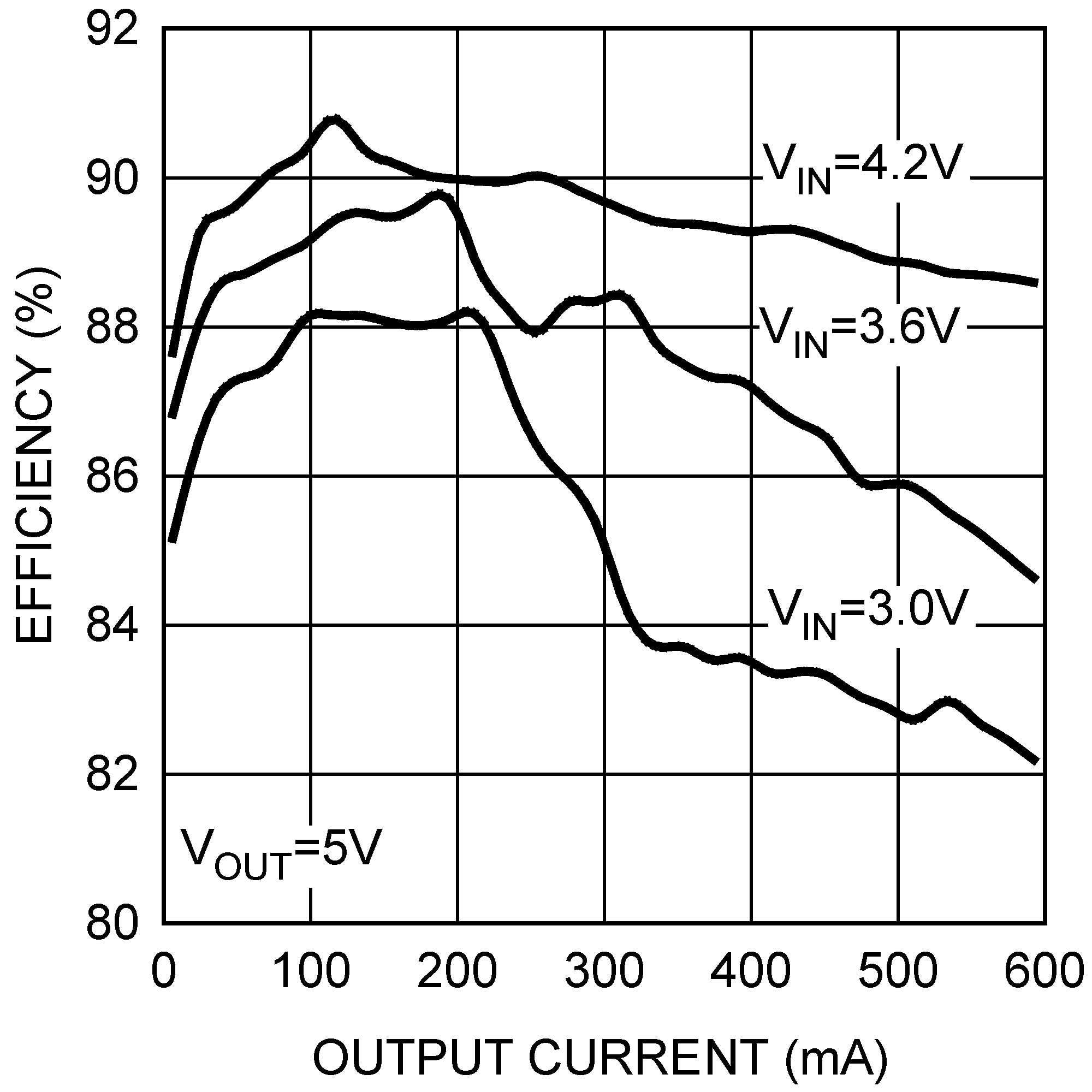
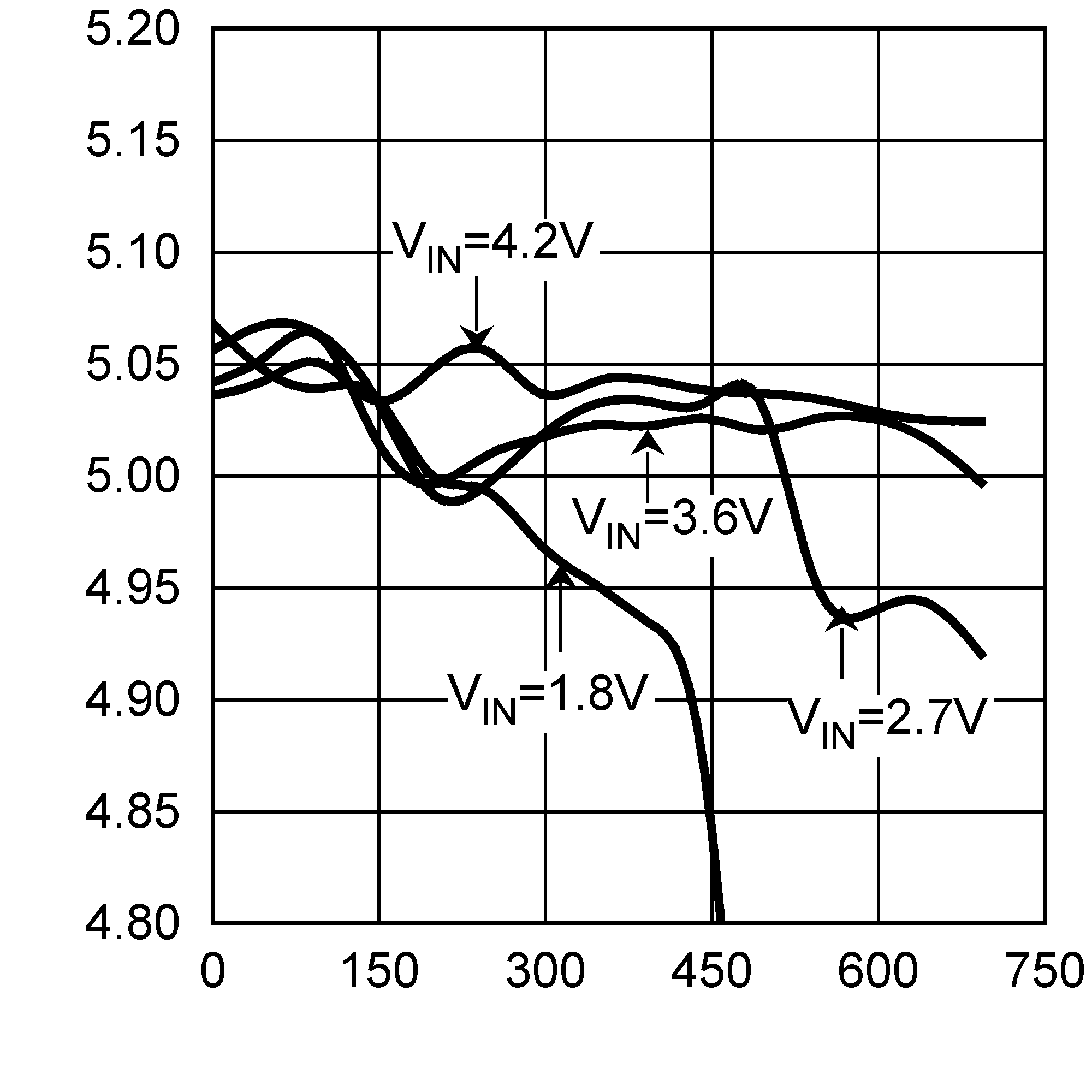
8.2.3 Application Curves


| VOUT = 5 V |