ZHCSGW9 October 2017 LM2623-Q1
PRODUCTION DATA.
6 Specifications
6.1 Absolute Maximum Ratings
over operating free-air temperature range (unless otherwise noted)(1) (2)| MIN | MAX | UNIT | ||
|---|---|---|---|---|
| Input pins | SW pin voltage | –0.5 | 14.5 | V |
| BOOT, VDD, EN, and FB pins | –0.5 | 10 | V | |
| FREQ pin | 100 | µA | ||
| Power dissipation (TA = 25°C)(3) | 500 | mW | ||
| TJ_MAX (3) | 150 | °C | ||
| Storage temperature, Tstg | –55 | 150 | °C | |
6.2 ESD Ratings
| VALUE | UNIT | ||||
|---|---|---|---|---|---|
| V(ESD) | Electrostatic discharge | Human body model (HBM), per AEC Q100-002(1) | All pins except 12 and 13 | ±2000 | V |
| Pins 12 and 13 | ±1000 | ||||
| Charged device model (CDM), per AEC Q100-011 | ±500 | ||||
6.3 Recommended Operating Conditions
over operating free-air temperature range (unless otherwise noted)| MIN | NOM | MAX | UNIT | ||
|---|---|---|---|---|---|
| Input pins | VDD pin | 3 | 5 | V | |
| FB and EN pins | 0 | VDD | V | ||
| BOOT pin | 0 | 10 | V | ||
| Operating junction temperature range, TJ | –40 | 125 | °C | ||
6.4 Thermal Information
| THERMAL METRIC(1) | LM2623-Q1 | UNIT | |
|---|---|---|---|
| NHL (WSON) | |||
| 14 PINS | |||
| RθJA | Junction-to-ambient thermal resistance | 37.6 | °C/W |
| RθJC(top) | Junction-to-case (top) thermal resistance | 26.9 | °C/W |
| RθJB | Junction-to-board thermal resistance | 15.0 | °C/W |
| ψJT | Junction-to-top characterization parameter | 0.3 | °C/W |
| ψJB | Junction-to-board characterization parameter | 4.7 | °C/W |
(1) For more information about traditional and new thermal metrics, see the Semiconductor and IC Package Thermal Metrics application report.
6.5 Electrical Characteristics
Limits apply for TJ = 25°C and VDD = VOUT = 3.3 V, unless otherwise specified.| PARAMETER | TEST CONDITIONS | MIN | TYP | MAX | UNIT | |
|---|---|---|---|---|---|---|
| GENERAL | ||||||
| VDD_ST | Start-up supply voltage 25°C | ILOAD = 0 mA(1) | 1.1 | V | ||
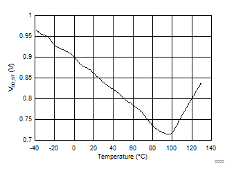
| VIN_OP | Minimum operating supply voltage (once started) | ILOAD = 0 mA | 0.65 | 0.9 | V | |
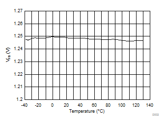
| VFB | FB pin voltage | 1.24 | V | |||
| –40°C to 85°C | 1.2028 | 1.2772 | ||||
| –40°C to 125°C | 1.2028 | 1.2772 | ||||
| VOUT_MAX | Maximum output voltage | 14 | V | |||
| η | Efficiency | VIN = 3.6 V; VOUT = 5 V, ILOAD = 500 mA | 87% | |||
| VIN = 2.5 V; VOUT = 3.3 V, ILOAD = 200 mA | 87% | |||||
| D | Switch duty cycle | 17% | ||||
| IDD | Operating quiescent current(2) | FB pin > 1.3 V, EN pin at VDD | 80 | µA | ||
| FB pin > 1.3 V, EN pin at VDD , –40°C to 85°C | 110 | |||||
| FB pin > 1.3 V, EN pin at VDD, –40°C to 125°C | 110 | |||||
| ISD | Shutdown quiescent current(3) | VDD, BOOT, and SW pins at 5 V, EN pin < 200 mV | 0.01 | µA | ||
| VDD, BOOT, and SW pins at 5 V, EN pin < 200 mV, –40°C to 85°C | 2.5 | |||||
| VDD, BOOT, and SW pins at 5 V, EN pin < 200 mV, –40°C to 125°C | 2.5 | |||||
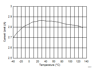
| ICL | Switch peak current limit | 2.2 | 2.85 | A | ||
| RDSON | MOSFET switch on resistance | 0.17 | Ω | |||
| –40°C to 85°C | 0.26 | |||||
| –40°C to 125° | 0.26 | |||||
| ENABLE SECTION | ||||||
| VEN_LO | EN pin voltage low(4) | –40°C to 85°C | 0.15 VDD | V | ||
| –40°C to 125°C | 0.15 VDD | |||||
| VEN_HI | EN pin voltage high(4) | –40°C to 85°C | 0.7 VDD | V | ||
| –40°C to 125°C | 0.7 VDD | |||||
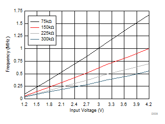
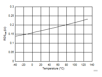
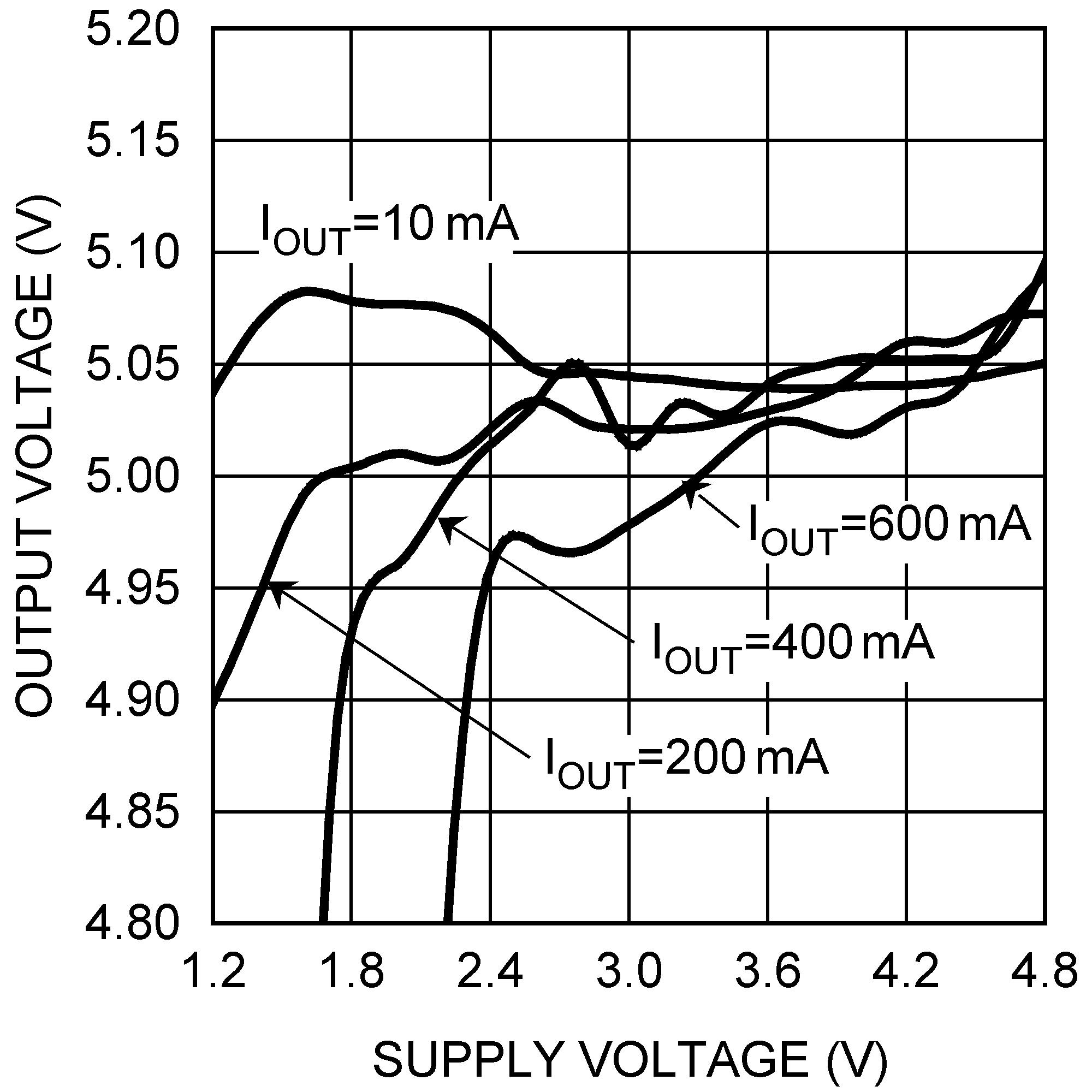
6.6 Typical Characteristics
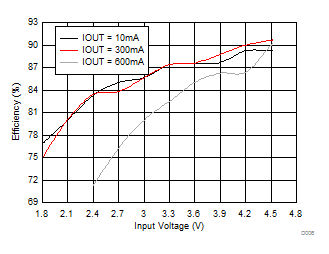
| VOUT = 5 V |
| VOUT = 5 V |
