ZHCSGW9 October   2017 LM2623-Q1

PRODUCTION DATA.  

  1. 特性
  2. 应用
  3. 说明
  4. 修订历史记录
  5. Pin Configuration and Functions
  6. Specifications
    1. 6.1 Absolute Maximum Ratings
    2. 6.2 ESD Ratings
    3. 6.3 Recommended Operating Conditions
    4. 6.4 Thermal Information
    5. 6.5 Electrical Characteristics
    6. 6.6 Typical Characteristics
  7. Detailed Description
    1. 7.1 Overview
    2. 7.2 Functional Block Diagram
    3. 7.3 Feature Description
      1. 7.3.1 Gated Oscillator Control Scheme
      2. 7.3.2 Cycle-To-Cycle PFM
      3. 7.3.3 Shutdown
      4. 7.3.4 Internal Current Limit and Thermal Protection
    4. 7.4 Device Functional Modes
      1. 7.4.1 Pulse Frequency Modulation (PFM)
      2. 7.4.2 Low Voltage Start-Up
  8. Applications and Implementation
    1. 8.1 Application Information
    2. 8.2 Typical Application
      1. 8.2.1 Design Requirements
      2. 8.2.2 Detailed Design Procedure
        1. 8.2.2.1 Non-Linear Effect
        2. 8.2.2.2 Choosing the Correct C3 Capacitor
        3. 8.2.2.3 Setting the Output Voltage
        4. 8.2.2.4 VDD Supply
        5. 8.2.2.5 Setting the Switching Frequency
        6. 8.2.2.6 Output Diode Selection
      3. 8.2.3 Application Curves
  9. Power Supply Recommendations
  10. 10Layout
    1. 10.1 Layout Guidelines
      1. 10.1.1 Boost Output Capacitor Placement
      2. 10.1.2 Schottky Diode Placement
      3. 10.1.3 Boost Input / VDD Capacitor Placement
    2. 10.2 Layout Example
    3. 10.3 WSON Package Devices
  11. 11器件和文档支持
    1. 11.1 器件支持
      1. 11.1.1 Third-Party Products Disclaimer
    2. 11.2 文档支持
      1. 11.2.1 相关文档
    3. 11.3 接收文档更新通知
    4. 11.4 社区资源
    5. 11.5 商标
    6. 11.6 静电放电警告
    7. 11.7 Glossary
  12. 12机械、封装和可订购信息

封装选项

机械数据 (封装 | 引脚)
散热焊盘机械数据 (封装 | 引脚)
订购信息

Pin Configuration and Functions

NHL Package
14-Pin WSON
Top View
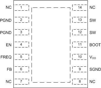
LM2623-Q1 Package_Drawing.gif

Pin Functions

PIN TYPE DESCRIPTION
NO. NAME
1 NC No connect
2, 3 PGND GND Power ground (pins 2 and 3 must be shorted together)
4 EN Digital Active-low shutdown input
5 FREQ Analog Frequency adjust; connect an external resistor between this pin and a voltage source sets the switching frequency of the LM2623-Q1.
6 FB Analog Output voltage feedback
7 NC No connect
8 NC No connect
9 SGND GND Signal ground
10 VDD Power Power supply for internal circuitry
11 BOOT Analog Bootstrap supply for the gate drive of internal MOSFET power switch
12, 13 SW Analog Drain of the internal MOSFET power switch (pins 12 and 13 must be shorted together)
14 NC No connect
DAP DAP Thermal Solder to board for enhanced thermal dissipation; must be electrically isolated/floating.