SNOSBH7F April 1999 – September 2014 LF412-N
PRODUCTION DATA.
1 Features
- Internally Trimmed Offset Voltage: 1 mV (Max)
- Input Offset Voltage Drift: 7 µV/°C (Typ)
- Low Input Bias Current: 50 pA
- Low Input Noise Current: 0.01 pA / √Hz
- Wide Gain Bandwidth: 3 MHz (Min)
- High Slew Rate: 10V/µs (Min)
- Low Supply Current: 1.8 mA/Amplifier
- High Input Impedance: 1012Ω
- Low Total Harmonic Distortion: ≤0.02%
- Low 1/f Noise Corner: 50 Hz
- Fast Settling Time to 0.01%: 2 µs
2 Applications
- High Speed Integrators
- Fast D/A Converters
- Sample and Hold Circuits
3 Description
These devices are low cost, high speed, JFET input operational amplifiers with very low input offset voltage and input offset voltage drift. They require low supply current yet maintain a large gain bandwidth product and fast slew rate. In addition, well matched high voltage JFET input devices provide very low input bias and offset currents. The LF412-N dual is pin compatible with the LM1558, allowing designers to immediately upgrade the overall performance of existing designs.
These amplifiers may be used in applications such as high speed integrators, fast D/A converters, sample and hold circuits and many other circuits requiring low input offset voltage and drift, low input bias current, high input impedance, high slew rate and wide bandwidth.
Device Information(1)
| PART NUMBER | PACKAGE | BODY SIZE (NOM) |
|---|---|---|
| LF412ACN | PDIP | 9.59 mm x 6.35 mm |
| LF412CN | PDIP | 9.59 mm x 6.35 mm |
| LF412MH | TO | 9.14 mm diameter |
- For all available packages, see the orderable addendum at the end of the datasheet.
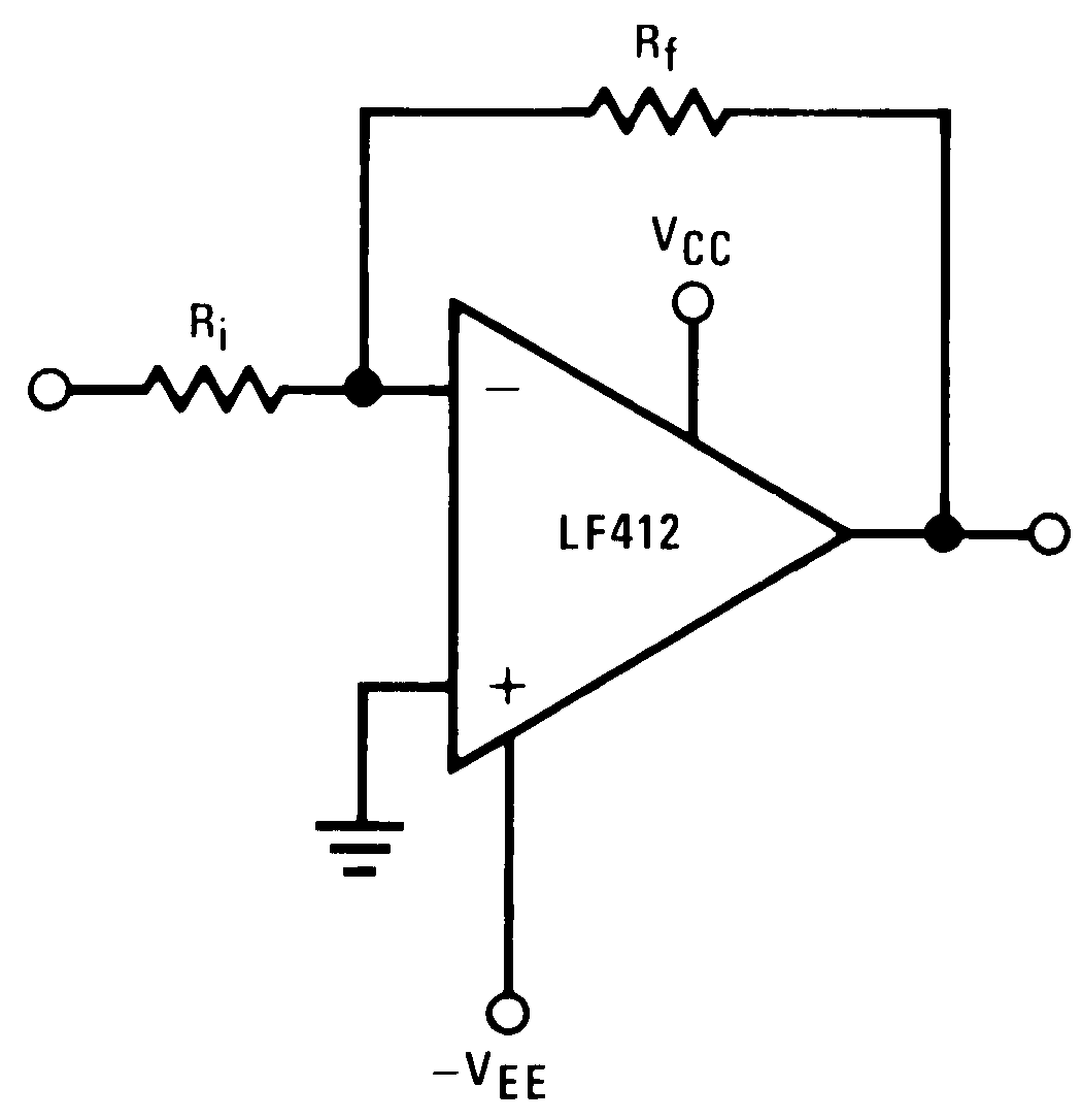
Inverting Amplifier