ZHCSDZ6D July 2012 – July 2015 DS90UB913Q-Q1 , DS90UB914Q-Q1
PRODUCTION DATA.
- 1 特性
- 2 应用
- 3 说明
- 4 修订历史记录
- 5 说明(续)
- 6 器件比较表
- 7 Pin Configuration and Functions
-
8 Specifications
- 8.1 Absolute Maximum Ratings
- 8.2 ESD Ratings
- 8.3 Recommended Operating Conditions
- 8.4 Thermal Information
- 8.5 Electrical Characteristics
- 8.6 Timing Requirements: Recommended for Serializer PCLK
- 8.7 AC Timing Specifications (SCL, SDA) - I2C Compliant
- 8.8 Bidirectional Control Bus DC Timing Specifications (SCL, SDA) - I2C Compliant
- 8.9 Switching Characteristics: Serializer
- 8.10 Switching Characteristics: Deserializer
- 8.11 Typical Characteristics
- 9 Parameter Measurement Information
-
10Detailed Description
- 10.1 Overview
- 10.2 Functional Block Diagram
- 10.3
Feature Description
- 10.3.1 Serial Frame Format
- 10.3.2 Line Rate Calculations for the DS90UB91xQ
- 10.3.3 Deserializer Multiplexer Input
- 10.3.4 Error Detection
- 10.3.5 Description of Bidirectional Control Bus and I2C Modes
- 10.3.6 Slave Clock Stretching
- 10.3.7 I2C Pass-Through
- 10.3.8 ID[x] Address Decoder on the Serializer
- 10.3.9 ID[x] Address Decoder on the Deserializer
- 10.3.10 Programmable Controller
- 10.3.11 Synchronizing Multiple Cameras
- 10.3.12 General-Purpose I/O (GPIO) Descriptions
- 10.3.13 LVCMOS VDDIO Option
- 10.3.14 Deserializer - Adaptive Input Equalization (AEQ)
- 10.3.15 EMI Reduction
- 10.4
Device Functional Modes
- 10.4.1 DS90UB91xQ-Q1 Operation With External Oscillator as Reference Clock
- 10.4.2 DS90UB91xQ-Q1 Operation With Pixel Clock from Imager as Reference Clock
- 10.4.3 MODE Pin on Serializer
- 10.4.4 MODE Pin on Deserializer
- 10.4.5 Clock-Data Recovery Status Flag (LOCK), Output Enable (OEN) and Output State Select (OSS_SEL)
- 10.4.6 Multiple Device Addressing
- 10.4.7 Powerdown
- 10.4.8 Pixel Clock Edge Select (TRFB / RRFB)
- 10.4.9 Power-Up Requirements and PDB Pin
- 10.4.10 Built-In Self Test
- 10.4.11 BIST Configuration and Status
- 10.5 Register Maps
- 11Application and Implementation
- 12Power Supply Recommendations
- 13Layout
- 14器件和文档支持
- 15机械、封装和可订购信息
11 Application and Implementation
NOTE
Information in the following applications sections is not part of the TI component specification, and TI does not warrant its accuracy or completeness. TI’s customers are responsible for determining suitability of components for their purposes. Customers should validate and test their design implementation to confirm system functionality.
11.1 Applications Information
The serializer and deserializer support only AC-coupled interconnects through an integrated DC-balanced decoding scheme. External AC-coupling capacitors must be placed in series in the FPD-Link III signal path as illustrated in Figure 45.
 Figure 45. AC-Coupled Connection
For high-speed FPD-Link III transmissions, the smallest available package should be used for the AC-coupling capacitor. This will help minimize degradation of signal quality due to package parasitics. The I/Os require a
100-nF AC-coupling capacitors to the line.
11.2 Typical Application
 Figure 46. Application Block Diagram
11.2.1 Design Requirements
11.2.1.1 Transmission Media
The DS90UB91xQ-Q1 chipset is intended to be used in a point-to-point configuration through a shielded twisted pair cable. The serializer and deserializer provide internal termination to minimize impedance discontinuities. The interconnect (cable and connectors) should have a differential impedance of 100 Ω. The maximum length of cable that can be used is dependent on the quality of the cable (gauge, impedance), connector, board (discontinuities, power plane), the electrical environment (for example, power stability, ground noise, input clock jitter, PCLK frequency, and so forth). The resulting signal quality at the receiving end of the transmission media may be assessed by monitoring the differential eye opening of the serial data stream. A differential probe should be used to measure across the termination resistor at the CMLOUTP/N pins. Figure 20 illustrates the minimum eye width and eye height that is necessary for bit error free operation.
11.2.1.2 Adaptive Equalizer – Loss Compensation
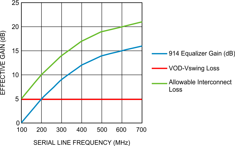
The adaptive equalizer is designed to compensate for signal degradation due to the differential insertion loss of the interconnect components. There are limits to the amount of loss that can be compensated – these limits are defined by the gain curve of the equalizer. In addition, there is an inherent tolerance for loss defined by the delta between the minimum VDO of the serializer and the input threshold (Vswing) of the deserializer. In order to determine the maximum cable reach, other factors that affect signal integrity such as jitter, skew, ISI, crosstalk, and so forth, need to be taken into consideration. Figure 49 illustrates the maximum allowable interconnect loss with the adaptive equalizer at its maximum gain setting (914 equalizer gain).
11.2.2 Detailed Design Procedure
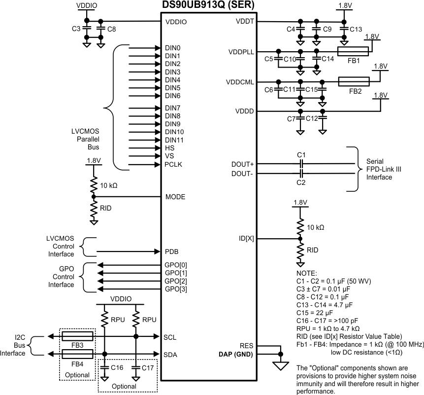
Figure 47 shows the typical connection of a DS90UB913Q-Q1 serializer.
 Figure 47. DS90UB913Q-Q1 Typical Connection Diagram — Pin Control
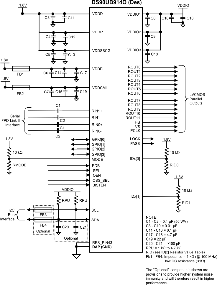
Figure 48 shows a typical connection of the DS90UB914Q-Q1 deserializer.
 Figure 48. DS90UB914Q-Q1 Typical Connection Diagram — Pin Control
11.2.3 Application Curve
 Figure 49. Adaptive Equalizer – Interconnect Loss Compensation