ZHCS016E January 2011 – July 2015 DRV8833
PRODUCTION DATA.
- 1 特性
- 2 应用
- 3 说明
- 4 修订历史记录
- 5 Pin Configuration and Functions
- 6 Specifications
- 7 Detailed Description
- 8 Application and Implementation
- 9 Power Supply Recommendations
- 10Layout
- 11器件和文档支持
- 12机械、封装和可订购信息
封装选项
请参考 PDF 数据表获取器件具体的封装图。
机械数据 (封装 | 引脚)
- PW|16
- RTY|16
- PWP|16
散热焊盘机械数据 (封装 | 引脚)
- PWP|16
订购信息
8 Application and Implementation
NOTE
Information in the following applications sections is not part of the TI component specification, and TI does not warrant its accuracy or completeness. TI’s customers are responsible for determining suitability of components for their purposes. Customers should validate and test their design implementation to confirm system functionality.
8.1 Application Information
The DRV8833 is used in brushed DC or stepper motor control. The following design procedure can be used to configure the DRV8833 in a brushed DC motor application. The inputs and outputs are connected in parallel to achieve higher current.
8.2 Typical Application
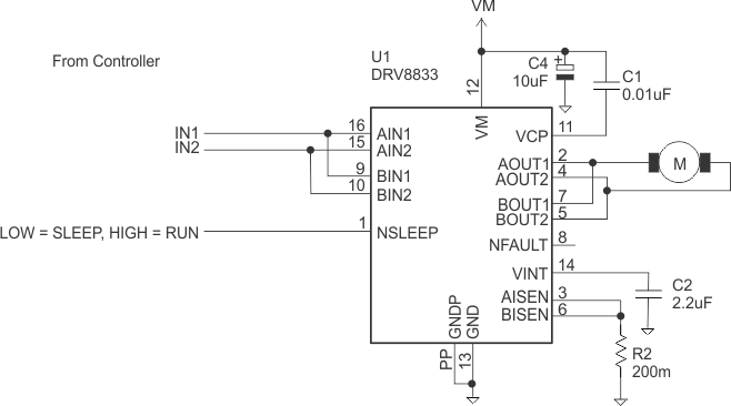
The two H-bridges in the DRV8833 can be connected in parallel for double the current of a single H-bridge. The internal dead time in the DRV8833 prevents any risk of cross-conduction (shoot-through) between the two bridges due to timing differences between the two bridges. Figure 7 shows the connections.
 Figure 7. Parallel Mode
8.2.1 Design Requirements
Table 5. Design Parameters
| DESIGN PARAMETER | REFERENCE | EXAMPLE VALUE |
|---|---|---|
| Motor voltage | VM | 10 V |
| Motor RMS current | IRMS | 0.8 A |
| Motor start-up current | ISTART | 2 A |
| Motor current trip point | ITRIP | 2.5 A |
8.2.2 Detailed Design Procedure
8.2.2.1 Motor Voltage
The motor voltage to use will depend on the ratings of the motor selected and the desired RPM. A higher voltage spins a brushed DC motor faster with the same PWM duty cycle applied to the power FETs. A higher voltage also increases the rate of current change through the inductive motor windings.
8.2.2.2 Motor Current Trip Point
When the voltage on pin xISEN exceeds VTRIP (0.2 V), current regulation is activated. The RISENSE resistor should be sized to set the desired ICHOP level.
To set ICHOP to 1 A, RSENSE = 0.2 V / 1 A = 0.2 Ω.
8.2.2.3 Sense Resistor
For optimal performance, it is important for the sense resistor to be:
- Surface-mount
- Low inductance
- Rated for high enough power
- Placed closely to the motor driver
The power dissipated by the sense resistor equals IRMS2 × R. For example, if peak motor current is 3 A, RMS motor current is 2 A, and a 0.05-Ω sense resistor is used, the resistor will dissipate 2 A2× 0.05 Ω = 0.2 W. The power quickly increases with higher current levels.
Resistors typically have a rated power within some ambient temperature range, along with a derated power curve for high ambient temperatures. When a PCB is shared with other components generating heat, margin should be added. For best practice, measure the actual sense resistor temperature in a final system, along with the power MOSFETs, as those are often the hottest components.
Because power resistors are larger and more expensive than standard resistors, the common practice is to use multiple standard resistors in parallel, between the sense node and ground. This distributes the current and heat dissipation.
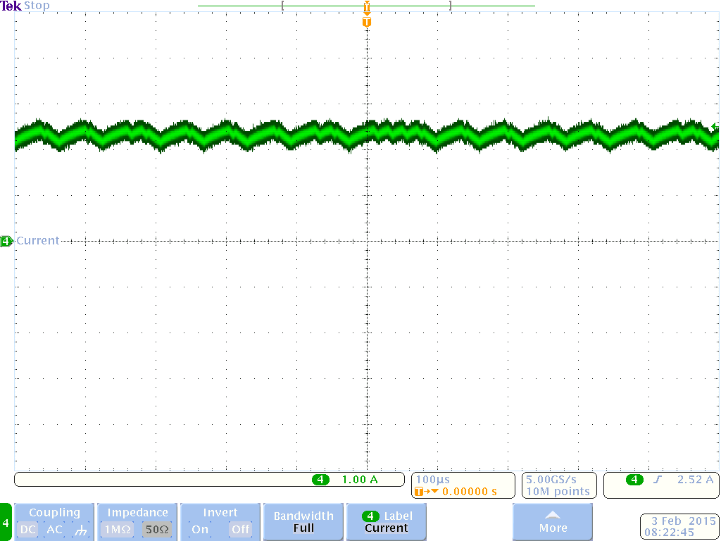
8.2.3 Application Curve
